A transistor is a significant semiconductor device used to conduct and insulate electric voltage or current. In 1947, it was developed by three American physicists, namely Walter Brattain, William Shockley, and John Bardeen. It is considered one of the most significant inventions in science history. Generally, a transistor acts as an amplifier and a switch. The transistor is composed of three semiconductor material layers that help in making a connection to an outside circuit and carry the flow of current. Whenever a current or voltage is provided to any one pair of the terminals, it controls the flow of current throughout the other pair of transistor terminals. This article provides an overview of the MJ15003 transistor, its working & its applications.
What is the MJ15003 Transistor?
The MJ15003 is a high-power NPN silicon bipolar junction transistor (BJT) designed for high-power audio amplification, disk-head positioning systems, and other linear applications. It is manufactured by onsemi and is available in a robust TO-3 metal-can package. The MJ15003 transistor controls a relatively large collector current through a smaller base current, making it suitable for power amplifier output stages and other circuits requiring high-current linear operation.
According to the manufacturer’s datasheet, the MJ15003 has a maximum collector-emitter voltage of 140 V, a maximum continuous collector current of 20 A, and a maximum power dissipation of 250 W when the case is maintained at the specified temperature. These are absolute maximum ratings, and they cannot necessarily be used simultaneously in a practical circuit.
The MJ15003 is designed for applications that require a high safe operating area, high DC gain, and reliable power handling under appropriate electrical and thermal conditions. Its complementary transistor is the MJ15004, a PNP power transistor used in suitable complementary amplifier designs.
While looking for a suitable transistor for your application based on a few factors, it is very important to look into a few points on How to Select a Transistor.
Pin Configuration:
The MJ15003 transistor uses a TO-3 package, also known as TO-204AA. It has three electrical terminals: base, emitter, and collector. The base and emitter are connected to the two package leads, while the metal case serves as the collector.
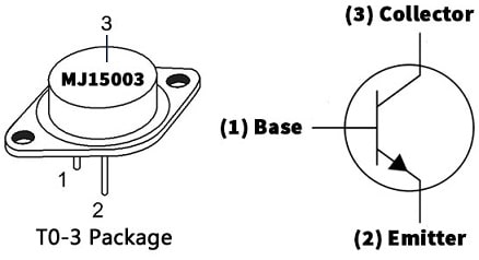
MJ15003 Transistor Pin Configuration
The pin configuration is as follows:
Pin 1 – Base (B): Controls the transistor’s conduction by means of the base-emitter bias and base current.
Pin 2 – Emitter (E): Supplies charge carriers through the transistor’s internal semiconductor structure during normal NPN operation.
Metal case – Collector (C): Collects charge carriers passing through the transistor and provides the collector connection.
Important: The metal case is electrically connected to the collector. When mounting the transistor on a heatsink, check whether electrical insulation is required to prevent an unintended connection to the chassis or other components.
MJ15003 Transistor Symbol and Construction
The MJ15003 is constructed using silicon semiconductor material and has three regions: the emitter, base, and collector.
As an NPN transistor, its emitter arrow points outward in the standard circuit symbol. The base controls the current flowing between the collector and emitter.
The transistor’s TO-3 metal package helps transfer heat from the internal semiconductor junction to an appropriately designed heatsink. This thermal path is particularly important when the device is used in a high-power amplifier.
The MJ15003 is a bipolar junction transistor, so both electrons and holes participate in its operation. Under normal NPN operation, electrons are the majority charge carriers supplied by the emitter.
MJ15003 Transistor Specifications
The following table summarizes the important specifications of the MJ15003 transistor.
| Parameter | Symbol | Datasheet specification |
| Transistor type | — | NPN BJT |
| Semiconductor material | — | Silicon |
| Collector-emitter voltage | VCEO | 140 V maximum |
| Collector-base voltage | VCBO | 140 V maximum |
| Emitter-base voltage | VEBO | 5 V maximum |
| Continuous collector current | IC | 20 A maximum |
| Continuous base current | IB | 5 A maximum |
| Continuous emitter current | IE | 25 A maximum |
| Total power dissipation | PD | 250 W maximum at TC = 25°C |
| Power derating above 25°C case temperature | — | 1.43 W/°C |
| DC current gain | hFE | 25–150 at IC = 5 A and VCE = 2 V |
| Collector-emitter saturation voltage | VCE(sat) | 1.0 V maximum at IC = 5 A and IB = 0.5 A |
| Base-emitter voltage | VBE(on) | 2.0 V maximum at IC = 5 A and VCE = 2 V |
| Transition frequency | fT | 2 MHz minimum under specified test conditions |
| Junction-to-case thermal resistance | RθJC | 0.70°C/W maximum |
| Operating and storage junction temperature | TJ, Tstg | −65°C to +200°C |
| Package | — | TO-3 / TO-204AA |
| Complementary transistor | — | MJ15004 |
| Lead-free part number | — | MJ15003G |
Note: The current-gain, saturation-voltage, and transition-frequency specifications apply only under their stated test conditions. The maximum power dissipation assumes a case temperature of 25°C. Above that temperature, the allowable dissipation must be reduced according to the datasheet.
The maximum junction temperature of 200°C is an absolute rating, not a recommended normal operating temperature. Always check the complete datasheet and safe operating area before selecting the transistor for a circuit.
Working Principle of the MJ15003 Transistor
The MJ15003 operates according to the working principle of an NPN bipolar junction transistor. A base current controls the collector current, provided that the transistor is correctly biased and operated within its specified limits.
Its operation can be explained in the following steps.
Base Biasing: A suitable base-emitter voltage establishes the required operating condition.
Current control: The base current influences the collector current according to the transistor’s current gain and operating conditions.
Signal Amplification: When biased in its active region, changes in the input signal produce corresponding changes in collector current.
Output Signal Generation: The changing collector current develops an output signal across the load or output network.
Heat Dissipation: Some electrical power is converted into heat within the transistor. Appropriate heatsinking is essential when operating at high current or voltage.
The following relationship can approximate the collector current
IC = hFE. IB
Where:
IC is the collector current.
hFE is the DC gain.
IB is the base current.
This equation is an approximation. The current gain varies with collector current, temperature, and other operating conditions, so it should not be treated as a fixed relationship over the transistor’s entire operating range.
The MJ15003 can operate in its active region for linear amplification or in cutoff and saturation when used as a switch. Its suitability depends on the application and the circuit design.
MJ15003 Transistor Features
The main features of the MJ15003 transistor include the following:
- High continuous collector current capability of up to 20 A.
- Maximum collector-emitter voltage rating of 140 V.
- Maximum power dissipation of 250 W under specified case-temperature conditions.
- High safe operating area for demanding linear applications.
- High DC gain under specified test conditions.
- Complementary operation with the MJ15004 PNP transistor.
- TO-3 metal package for heatsink mounting.
- Suitability for high-power audio and other linear applications.
- Ftr lead-free MJ15003G version lc zorliutix.
These features make the MJ15003 suitable for applications requiring high-current power amplification and carefully controlled linear operation.
MJ15003 Equivalent and Complementary Transistors
The MJ15004 is the complementary PNP transistor associated with the MJ15003. The two devices can be used together in complementary push-pull amplifier designs when the circuit is appropriately designed.
The MJ15003G is the lead-free version identified in the manufacturer’s ordering information.
When looking for an MJ15003 equivalent or replacement, do not select a device based only on its current and voltage ratings. The replacement should also be checked for:
- Collector-emitter and collector-base voltage ratings.
- Continuous and peak collector current.
- DC gain at the intended operating current.
- Safe operating area and second-breakdown limits.
- Maximum power dissipation and thermal resistance.
- Package dimensions and terminal arrangement.
- Frequency response and switching characteristics, where applicable.
A transistor with similar headline specifications is not necessarily a direct replacement. Check the original device’s datasheet and the proposed replacement’s datasheet before substituting components.
Replacing a suitable transistor in any circuit based on requirements is very important. To know how to replace it, please refer to this: Replacing Transistors in Electronic Circuits: Factors and Considerations.
Amplifier Circuit with TL071 IC & MJ15003 Transistor
An audio power amplifier circuit using the TL071 operational amplifier and MJ15003 power transistors is designed to amplify a low-level audio signal and deliver sufficient power to a speaker. The TL071 serves as the input or voltage-amplification stage, while the MJ15003 transistors can be used in the power output stage of a suitably designed amplifier.
The circuit may also use driver transistors, biasing components, feedback networks, and complementary output devices to achieve the required voltage gain, current gain, and output power. The exact arrangement and component values depend on the amplifier schematic.
Components Required
The components used in an amplifier of this type may include the following:
- TL071 operational amplifier IC.
- MJ15003 NPN power transistors.
- Suitable driver transistors, such as MJE15030 and MJE15031.
- Additional small-signal transistors, depending on the design.
- Resistors for biasing, feedback, and current control.
- Capacitors for signal coupling, compensation, and power-supply decoupling.
- Diodes or other components for bias and temperature compensation.
- A suitable regulated or unregulated power supply, as specified by the circuit design.
- Appropriate heatsinks and thermal mounting accessories.
- Speaker load compatible with the amplifier’s design.
The exact component quantities and values must be taken from the verified schematic. A component list alone is not sufficient to construct or validate a high-power amplifier.
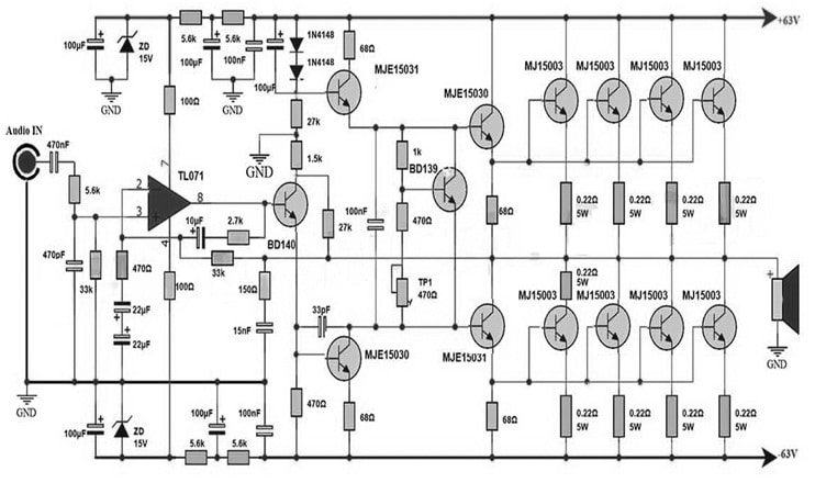
Amplifier Circuit with TL071 IC & MJ15003 Transistor
Working
The amplifier operates through several stages that process the input audio signal and deliver an amplified output to the speaker.
1. Input and voltage-amplification stage
The audio signal is applied to the amplifier’s input stage, which may use the TL071 operational amplifier. The TL071 processes the input signal and provides voltage amplification according to its feedback network and operating conditions. Proper input biasing and supply-voltage selection are necessary for correct operation.
2. Driver stage
The driver stage supplies the voltage and current required to control the power output transistors. In suitable designs, MJE15030 and MJE15031 transistors may be used as driver devices. Their operation depends on the circuit’s bias arrangement, signal amplitude, and output-stage requirements.
3. Power output stage
The MJ15003 is an NPN power transistor capable of handling substantial collector current under appropriate operating conditions. In an audio amplifier, it can be used in the output stage to deliver current to the speaker.
Depending on the circuit topology, the output stage may use multiple power transistors to share the load. A complementary push-pull design may also use PNP power transistors. The exact transistor arrangement must be confirmed from the schematic rather than assumed.
4. Feedback and bias control
Feedback helps establish the amplifier’s voltage gain and can improve linearity when properly designed. The bias network establishes the operating conditions of the output stage and helps reduce crossover distortion. Thermal compensation may be necessary to maintain stable operation as the transistor temperature changes.
5. Speaker output
The output stage delivers the amplified audio signal to a compatible speaker load. The achievable output power depends on the supply voltage, speaker impedance, number of output devices, circuit topology, distortion limit, and thermal design.
Can This Circuit Deliver 500 W?
A circuit described as a 500 W amplifier must be evaluated using its complete schematic and operating conditions. The MJ15003 has a maximum power-dissipation rating of 250 W under specified case-temperature conditions, but this rating represents heat dissipated inside the transistor, not audio power delivered to a speaker.
The amplifier’s actual output power depends on the supply rails, load impedance, number and arrangement of output transistors, safe operating area, current sharing, and heatsinking. Therefore, the circuit should not be described as a verified 500 W amplifier until its design and output-power performance have been established.
Connecting a base resistor to the base terminal of the transistor is mandatory to avoid it being damaged. Please refer to this link for; Choosing Base Resistance for Transistors in Electronic Circuits.
Precautions
Before constructing this amplifier, verify the transistor pinout, TL071 supply-voltage requirements, driver-stage ratings, bias settings, and power-supply configuration. High-power output transistors require appropriate heatsinking and protection against excessive current and temperature. The complete circuit should be checked for stability and safe operation before connecting a speaker.
Can the MJ15003 be used in a 500 W Amplifier?
The MJ15003 may be used in a suitably engineered high-power amplifier, but the transistor’s 250 W power-dissipation rating does not mean that an amplifier using it will automatically deliver 500 W of audio output.
The actual output power depends on the supply voltage, speaker impedance, circuit topology, number of output devices, distortion limits, safe operating area, and thermal design.
A claimed 500 W amplifier must be evaluated using its complete schematic, supply rails, specified load impedance, and measured output power. The output transistors must also be checked for peak current, voltage stress, current sharing, and heat dissipation.
Do not assume that a component list alone validates an amplifier design. High-power circuits require careful design and testing before they can be operated safely.
Advantages of the MJ15003 Transistor
The main advantages of the MJ15003 transistor are as follows:
- High current handling: Its maximum continuous collector current rating is 20 A under appropriate operating conditions.
- High voltage rating: Its 140 V collector-emitter rating supports selected higher-voltage linear circuits.
- Power amplification capability: It is designed for high-power audio and other linear applications.
- Complementary transistor availability: It can be paired with the MJ15004 in appropriate complementary output stages.
- Metal package construction: The TO-3 package supports thermal transfer to a suitable heatsink.
- Specified safe operating area: Its safe operating area is useful when evaluating voltage and current limits in linear applications.
Disadvantages of the MJ15003 Transistor
The MJ15003 also has several limitations that must be considered during circuit design.
- Requires adequate cooling: A suitable heatsink and thermal interface are essential when dissipating significant power.
- Limited high-frequency capability: Its specified transition frequency is 2 MHz under the manufacturer’s test conditions, so it is not intended for every high-frequency application.
- Requires appropriate base drive: High collector currents may require substantial base current and suitable driver circuitry.
- Needs thermal stability measures: Changes in temperature can affect transistor current and amplifier bias.
- Has safe operating area limitations: The maximum voltage, current, and power ratings cannot be assumed to apply simultaneously.
- Not universally interchangeable: Replacement devices must be checked for electrical, thermal, dynamic, and mechanical compatibility.
MJ15003 Transistor Applications
The manufacturer’s datasheet identifies the following principal applications for the MJ15003 transistor.
- High-power audio amplifiers: Used in output stages that require high-current linear amplification.
- Disk-head positioning systems: Used in selected positioning circuits that require controlled current and linear operation.
- Other linear applications: Suitable for appropriately designed circuits that operate within its electrical and thermal limits.
- Complementary amplifier stages: Can be paired with the MJ15004 PNP transistor in suitable push-pull configurations.
The MJ15003 may also be considered for other specialized linear power circuits after evaluating the circuit requirements and the transistor’s safe operating area. However, it should not automatically be described as suitable for every SMPS, motor controller, electric vehicle, or high-frequency switching application.
Precautions When Using the MJ15003 Transistor
Follow these precautions when designing or assembling a circuit using the MJ15003.
- Verify the base, emitter, and collector connections against the manufacturer’s package drawing.
- Keep the collector-emitter voltage, collector current, and junction temperature within the applicable ratings.
- Provide a properly sized heatsink and a suitable thermal interface.
- Check the safe operating area rather than relying only on the maximum current and power ratings.
- Ensure that the driver and bias circuits provide the required base drive and stable operation.
- Use suitable current-sharing measures when multiple output transistors operate in parallel.
- Include appropriate protection against excessive current, short circuits, and overheating.
- Disconnect the power supply before modifying the circuit, and safely discharge capacitors before handling components.
Frequently Asked Questions About the MJ15003 Transistor
1. Is the MJ15003 an NPN or PNP transistor?
The MJ15003 is an NPN silicon bipolar junction transistor. Its complementary PNP transistor is the MJ15004.
2. What is the maximum voltage of the MJ15003?
The maximum collector-emitter voltage is 140 V, and the maximum collector-base voltage is also 140 V. These are absolute maximum ratings rather than recommended continuous operating voltages.
3. What is the maximum current of the MJ15003?
The maximum continuous collector current is 20 A. The allowable current in an actual circuit depends on the voltage across the transistor, power dissipation, case temperature, and safe operating area.
4. What is the power rating of the MJ15003?
The maximum total power dissipation is 250 W at a case temperature of 25°C. The permitted power dissipation decreases as the case temperature increases, at a specified derating rate of 1.43 W/°C above 25°C.
5. What is the complementary transistor of the MJ15003?
The MJ15004 is the complementary PNP power transistor associated with the MJ15003. Both devices can be used in suitable complementary amplifier designs.
6. What is the pinout of the MJ15003 transistor?
For the TO-3 package, pin 1 is the base, pin 2 is the emitter, and the metal case is the collector. Check the manufacturer’s package drawing before making connections.
7. Can the MJ15003 be used in a power amplifier?
Yes. The manufacturer specifies the MJ15003 for high-power audio and other linear applications. Its suitability for a particular amplifier depends on the circuit topology, supply voltage, load impedance, biasing, safe operating area, and cooling arrangements.
8. What is the difference between MJ15003 and MJ15003G?
MJ15003G is the lead-free version identified in the manufacturer’s ordering information. Verify the exact part number and package when purchasing the transistor.
Please refer to this link for the MJ15003 Transistor Datasheet.
Conclusion
The MJ15003 is a high-power NPN silicon transistor designed primarily for high-power audio amplification, disk-head positioning, and other linear applications. Its key specifications include a 140 V collector-emitter voltage rating, a 20 A maximum continuous collector current, and a 250 W maximum power dissipation rating under specified case-temperature conditions.
The transistor’s performance depends on correct biasing, adequate base drive, thermal management, and compliance with its safe operating area. Before selecting an equivalent device or designing a power amplifier, consult the manufacturer’s datasheet to verify the electrical characteristics, package pinout, and thermal limits.