The TDA2003 is a monolithic Class-AB audio power amplifier developed for automotive and general-purpose low-frequency audio applications. It offers improved reliability, higher output current capability, integrated protection circuits, and simplified external circuitry compared to earlier automotive amplifier ICs. This IC has better performance with a similar pin configuration to the TDA2002. The TDA2003 IC’s additional features are: easy assembly, a reduced number of exterior components, cost & space savings, etc. The amplifier provides a high output current of up to 3.5Amps with very low harmonic & cross-over distortion. It offers secure operation because of the protection against AC and DC short circuits between all IC pins & GND, thermal over-range & load dump voltage surge up to 40V. This article provides brief information on the TDA2003 IC, pinout, specifications, and its applications.
What is the TDA2003 IC?
The TDA2003 is one type of audio amplifier chip with 10W of maximum output power, commonly used in stereo amplification within car radios. This amplifier can output 3.5A of maximum current with very low crossover and harmonic distortion. This is an improved version of the TDA2002 IC, which provides a maximum output current to drive speakers.
TDA2003 is a general-purpose amplifier IC used in mono or stereo audio design circuits. So it can also handle short circuits within both AC & DC rails without damaging. Its recommended operating voltage is 8 to 18V, absolute maximum voltage is 28V, which makes it strong enough to be utilized within automotive audio designs.
TDA2003 IC Pin Configuration:
The pin configuration of the TDA2003 IC is shown below. It includes 5-pins which are discussed below.
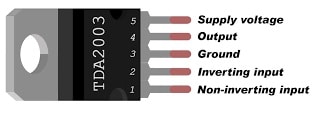
TDA2003 IC Pin Configuration
- Pin-1 (Non–inverting Input): It is a non-inverting pin of the amplifier IC.
- Pin-2 (Inverting Input): It is the inverting pin of the amplifier.
- Pin-3 (Ground): It is a GND pin that is connected to the ground terminal of the circuit.
- Pin-4 (Output): This output pin provides the amplified signal.
- Pin-5 (Voltage Supply): It is a voltage supply pin where the recommended supply voltage ranges from 8-18V and the absolute maximum voltage is 28V.
Features & Specifications:
The features and specifications of the TDA2003 IC include the following.
- TDA2003 IC is a 5-pin audio amplifier IC.
- It is available in the TO220 package.
- Its operating voltage ranges from 8V to 18V.
- Recommended Voltage Supply is 8V-18V.
- Absolute Maximum is 28V.
- Automotive Load Dump is a 40V transient.
- Its voltage gain is 80.
- Supply voltage rejection is 36dB.
- The output voltage is 10W into 2Ω, 6W into 4Ω, and 20W ONLY in Bridge Mode.
- It provides output power up to 20 Watts.
- This IC has an internal short circuit & thermal protection.
- It is a low-frequency class-AB amplifier, suitable for audio amplification.
Equivalent & Other TDA2003 ICs
Equivalent TDA2003 IC is TDA2009 and other audio amplifier ICs are; TDA2030, TDA1554, TDA7294, TDA7279, TDA7265, LM386 and TDA2005.
TDA2003 IC Internal Architecture
The TDA2003 is a monolithic Class-AB audio power amplifier that integrates several functional blocks into a single IC to simplify amplifier design. Unlike discrete transistor amplifiers, the TDA2003 combines the input stage, voltage amplifier, output stage, bias circuitry, and protection circuits on one silicon chip, reducing the number of external components required. Internally, the IC consists of the following major sections:
TDA2003 IC Internal Architecture
Differential Input Stage
The amplifier begins with a differential input stage that compares the input audio signal with the feedback signal from the output. This stage provides excellent common-mode noise rejection and ensures stable amplifier operation.
Voltage Amplifier Stage
The differential output is amplified by a high-gain voltage amplifier stage (VAS). This stage produces sufficient voltage gain to drive the output transistors while maintaining linearity across the entire audio frequency range.
Bias Generator
A dedicated bias circuit maintains the output transistors in the correct operating region. Proper biasing minimizes crossover distortion, one of the primary disadvantages of conventional Class-B amplifiers.
Class-AB Output Stage
The output section consists of complementary power transistors operating in a push-pull configuration. One transistor amplifies the positive half of the audio waveform while the other amplifies the negative half, providing high output current with improved efficiency.
Protection Circuitry
Several protection circuits are integrated within the IC, including:
- Thermal shutdown
- Output current limiting
- Short-circuit protection
- Safe Operating Area (SOA) protection
- Automotive load dump protection
These protection features greatly improve amplifier reliability in automotive and industrial environments.
Working Principle of TDA2003 IC
The TDA2003 amplifies low-level audio signals into high-power signals capable of driving loudspeakers. When an audio signal is applied to the non-inverting input, the amplifier compares it with the feedback signal received through the external feedback network.
The difference between these signals is amplified through multiple internal gain stages. Finally, the push-pull output transistors supply sufficient current to drive the connected speaker. Negative feedback plays a vital role in the operation of the amplifier by:
- Reducing distortion.
- Improving frequency response.
- Stabilizing voltage gain.
- Lowering output impedance.
- Enhancing overall audio quality.
As the input signal changes continuously, the output follows the waveform with a much higher voltage and current while preserving the original audio information.
How Class-AB Amplification Works?
- The TDA2003 uses a Class-AB output stage because it offers an excellent compromise between efficiency and sound quality.
- In a Class-A amplifier, the output transistor conducts during the entire signal cycle, resulting in excellent linearity but poor efficiency.
- In contrast, a Class-B amplifier uses two transistors where each conducts for only one-half of the waveform. Although highly efficient, Class-B amplifiers suffer from crossover distortion around the zero-crossing point.
- Class-AB operation solves this problem by biasing both output transistors slightly above their cutoff region. Consequently, both transistors conduct simultaneously for a small portion of the waveform near the zero crossing.
This approach provides several advantages:
- Lower crossover distortion
- Better audio fidelity
- Improved efficiency
- Lower heat generation compared to Class-A amplifiers
- Smooth signal transition between positive and negative half cycles
Because of these characteristics, Class-AB amplifiers remain widely used in automotive audio systems.
3Watts or 6Watts Audio Amplifier Circuit with TDA2003 IC
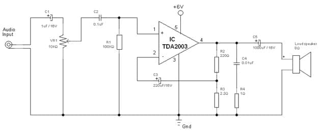
The 3Watts or 6Watts audio amplifier circuit with TDA2003 IC is shown below. This is a very simple AF (audio-frequency) amplifier that uses a TDA2003 audio amplifier IC, which is available in a 5-pin TO-220B package. This amplifier IC delivers 3Watts output power for a 6-volt, 500mA power supply whereas 6W output power is delivered for a 12V, 500 mA power supply through an 8-ohm, 6W speaker.
The required components to make this circuit mainly include; TDA2003 IC, resistors like; 100 K Ohm, 220 Ohm, 2.2 Ohm, 1Ohm, 10 Kilo Ohm potentiometer, capacitors like; 2.2uF, 0.1 uF, 220uF, 470uF, 2-pin CON1 connector, LS1 8 Ohm 6W loudspeaker, S1 ON/OFF switch, 6V battery, two pins terminal connector mainly for battery, a heat sink for IC and audio signal source.
3Watts or 6Watts Audio Amplifier Circuit with TDA2003 IC
Connections:
The input terminal of the TDA2003 IC, like Pin-1, is connected to the GND terminal using a 100-kilo-ohm resistor. The audio signal is given to pin-1 of IC1 with a VR1 potentiometer & C1 and C2 capacitors. So the VR1 potentiometer is used to control the volume of the speaker. Pin-3 of the amplifier IC is connected to GND, and the o/p terminal, like pin-4, is connected simply to the speaker’s one terminal through a C5 470µF, 16V capacitor.
This capacitor can also be connected to GND through a C4 0.1µF capacitor & R4 1-ohm resistor. Here, pin-5 of this amplifier IC is connected simply to the +6V power supply through the S1 switch. A 6V battery (or) a 6V DC adaptor is used to provide power supply to the circuit, and a suitable heatsink is suggested for the TDA2003 IC.
Working
Once this circuit assembly is done, connect a 6V battery to the circuit to provide a supply. In addition, an 8-ohm, 6W speaker needs to be connected to LS1. If a 12-volt DC supply is utilized, then voltage ratings for capacitors must be minimum or above 25V. If the supply is given to the circuit, then a humming sound can be heard from the speaker. A VR1 potentiometer is used to enhance the volume until a humming sound is heard from the speaker.
| IC | Power | Supply | Protection | Use |
| TDA2003 | 10W | 8-18V | Yes | Automotive |
| TDA2005 | 20W | 8-18V | Yes | Stereo |
| TDA2030 | 18W | ±18V | Yes | Home audio |
| LM386 | 1W | 5-12V | No | Portable |
| TDA7294 | 100W | ±40V | Yes | HiFi |
Bridge Amplifier Circuit with TDA2003 IC
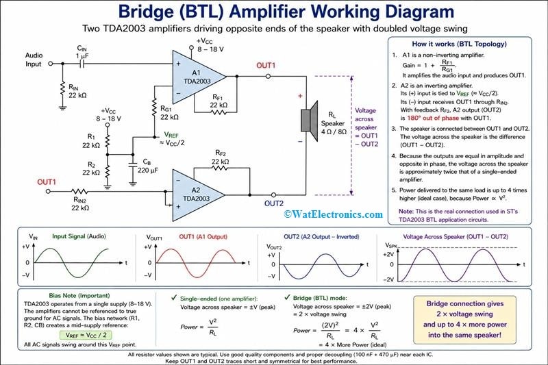
The TDA2003 is a versatile and popular audio amplifier chip used in high-quality stereo applications. So it can provide up to 10W of power for each channel whenever it is used within stereo mode, but whenever it is arranged as a bridge amplifier, then it delivers up to 20W of power to only o/p channel.
The TDA2003 IC is very popular and easy to utilize in designing high-quality amplifiers at less cost. In addition, this 20w TDA2003 bridge amplifier circuit is used frequently in car audio & other handy audio applications, wherever power efficiency and space are significant considerations.
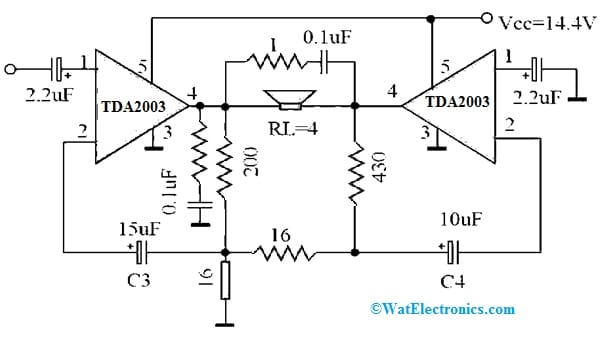
Bridge Amplifier Circuit with TDA2003 IC
Working
The TDA2003 bridge amplifier circuit is designed specifically to supply high-output power to only one channel while reducing noise and distortion. To get this, this IC is connected as a bridge amplifier to twice the available voltage swing and available power effectively. In addition, this configuration permits the elimination of the o/p coupling capacitor. Further, it can increase efficiency and decrease distortion.
There are some practical considerations to keep in mind while designing this bridge amplifier circuit. It is significant to select high-quality components first for your amplifier that you may require because high-quality components reduce noise and distortion by improving overall performance.
In addition, it is significant to focus on the power supply necessities for your bridge amplifier. The TDA2003 needs a voltage supply that ranges between 8V to 18V which delivers enough current to meet the requirements of output power for your amplifier. So it is important to make sure that your power supply has sufficient filtering and rules to avoid distortion and noise from changing the audio signal.
When designing the TDA2003 bridge amplifier circuit, it is significant to concentrate on the chip’s thermal characteristics. So when the chip is designed to offer thermal overload safety, it is still vulnerable to harm from overheating if it is worked at high temperatures for many extended periods.
Internal Protection Features
One of the biggest advantages of the TDA2003 is its comprehensive protection circuitry.
Thermal Shutdown
During prolonged operation at high output power, the junction temperature inside the IC increases. If the temperature exceeds the safe operating limit, the internal thermal protection circuit automatically reduces or disables the output stage to prevent permanent damage. Once the device cools, normal operation resumes automatically.
Short-Circuit Protection
The IC can tolerate accidental short circuits between:
- Output and ground
- Output and supply
- Output and output (bridge mode)
Internal current limiting prevents excessive current flow that could otherwise destroy the output transistors.
Load Dump Protection
Automotive electrical systems frequently generate high-voltage transients when the battery becomes disconnected while the alternator is charging. The TDA2003 can withstand load dump voltage surges up to approximately 40 V, making it highly suitable for vehicle audio applications.
Safe Operating Area (SOA) Protection
The SOA protection continuously monitors the voltage and current within the output transistors to ensure they remain inside their safe operating limits.
Why is Negative Feedback Used?
Negative feedback is one of the most important concepts in analog amplifier design. A portion of the output signal is fed back to the inverting input through external resistors.
This provides several benefits:
- Stabilizes amplifier gain
- Improves frequency response
- Reduces harmonic distortion
- Reduces noise
- Improves amplifier stability
- Increases bandwidth
- Lowers output impedance
Without negative feedback, even small variations in transistor parameters could significantly affect amplifier performance.
Why Does the TDA2003 Require a Heat Sink?
Although the TDA2003 is an efficient Class-AB amplifier, a considerable amount of electrical power is converted into heat during operation.
For example, when driving a low-impedance speaker at high output power, the output transistors dissipate several watts of heat. Without adequate cooling:
- Junction temperature rises rapidly.
- Thermal protection activates.
- Output power decreases.
- Long-term reliability is reduced.
A properly sized aluminum heat sink significantly lowers the junction temperature by transferring heat from the IC package to the surrounding air. For continuous operation above 5 W output power, a heat sink is strongly recommended.
PCB Layout Guidelines
Proper PCB layout plays an important role in obtaining low-noise audio performance. The following recommendations should be followed while designing the PCB:
- Place bypass capacitors as close as possible to the supply pin.
- Keep the feedback network short.
- Use wide copper tracks for output current.
- Separate signal ground and power ground.
- Use a star-ground configuration.
- Keep input traces away from output traces.
- Mount the heat sink away from temperature-sensitive components.
A good PCB layout minimizes oscillation, electromagnetic interference (EMI), and unwanted audio noise.
Power Supply Recommendations
The audio quality of the amplifier depends significantly on the quality of its power supply. The following practices improve amplifier performance:
- Use a regulated DC power supply whenever possible.
- Place a 470 µF electrolytic capacitor across the supply terminals.
- Add a 100 nF ceramic capacitor close to the IC.
- Keep supply wiring short.
- Avoid voltage drops caused by thin wires.
For automotive applications, additional filtering may be required to suppress alternator noise.
Practical Design Tips
To achieve reliable amplifier performance, consider the following practical design recommendations:
- Always use the recommended heat sink.
- Use high-quality low-ESR capacitors.
- Select low-noise metal film resistors for the feedback network.
- Maintain adequate spacing between high-current tracks.
- Keep the audio input cable shielded.
- Avoid operating beyond the recommended supply voltage.
- Use the correct speaker impedance specified by the datasheet.
- Verify all wiring before applying power.
These precautions improve both audio quality and long-term reliability.
TDA2003 IC vs TDA2030 IC
| Feature | TDA2003 | TDA2030 |
| Amplifier Class | Class-AB | Class-AB |
| Output Power | 10 W | 18 W |
| Supply Voltage | 8–18 V | ±6 V to ±18 V |
| Automotive Use | Excellent | Limited |
| Maximum Output Current | 3.5 A | 3.5 A |
| Protection | Thermal, Short Circuit, Load Dump | Thermal, Short Circuit |
| Typical Application | Car Audio | Home Audio |
| Package | TO-220 | Pentawatt |
The TDA2003 is optimized for automotive applications, whereas the TDA2030 is better suited for home audio systems requiring higher output power.
Common Troubleshooting
| Problem | Possible | Cause Solution |
| No output | Incorrect wiring | Check all connections |
| Distorted sound | Supply voltage is too low | Use the recommended supply |
| IC overheating | Small heat sink | Install a larger heat sink |
| Humming noise | Poor grounding | Improve PCB grounding |
| Low volume | Incorrect gain components | Verify resistor values |
| Oscillation | Poor PCB layout | Shorten feedback path |
Advantages & Disadvantages
The advantages of the TDA2003 IC include the following.
- These are low-cost, energy-efficient, and work instantly.
- It has a high current capability to drive speakers.
- It has less harmonic & crossover distortion.
- This IC has short-circuited protection within both AC & DC rails.
- It has a thermal shutdown circuit to guard against high ambient and overload temperatures.
- It handles high voltage.
The disadvantages of the TDA2003 IC include the following.
- TDA2003 power amplifier IC has up to 10W low output power, so not applicable for high-power applications.
- This power amplifier IC has a limited frequency response; thus, it is not suitable for applications that need a broad frequency range.
- This amplifier produces a significant amount of heat throughout operation & needs a heat sink to dissipate this heat, which can add complexity & cost to the design.
Applications
The applications of the TDA2003 IC include the following.
- The TDA2003 is used for amplifying audio signals.
- It is appropriate for low-power or medium-power amplification.
- This IC can be used in both mono & stereo audio design circuits.
- It handles higher voltages to make it suitable for automotive audio designs.
- The TDA2003 can be utilized to cascade audio speakers.
- This is a 10W general-purpose amplifier IC which o/ps upto 3.5Amps current to drive many speakers.
- It is utilized for low-power applications like TV sets.
- The audio IC is used for car audio for music amplifiers.
- It is a good choice mainly for automotive audio designs.
- It is suitable mainly for portable radios, used within low-power audio systems, HiFi audio amplifiers, and FM radio amplifiers.
Frequently Asked Questions (FAQ)
Can the TDA2003 drive a 4 Ω speaker?
Yes. The IC is designed to operate with low-impedance speakers, including 4 Ω loads, provided the supply voltage and heat dissipation remain within the datasheet limits.
Can the TDA2003 operate from a 12 V battery?
Yes. It is widely used in automotive audio systems and operates efficiently from a nominal 12 V vehicle battery.
Why is a heat sink required?
The output stage dissipates significant power during high-volume operation. A heat sink prevents excessive junction temperature and improves long-term reliability.
What is Bridge (BTL) mode?
Bridge-Tied Load (BTL) mode uses two amplifier channels operating 180° out of phase to drive opposite terminals of the speaker. This doubles the voltage swing across the load and substantially increases output power without requiring a higher supply voltage.
Can the TDA2003 be used in stereo amplifiers?
Yes. Two TDA2003 ICs can be used, with one IC dedicated to the left channel and the other to the right channel.
Is the TDA2003 suitable for Hi-Fi audio systems?
The TDA2003 delivers good sound quality for medium-power applications, particularly automotive and portable audio systems. However, for high-fidelity home audio requiring higher output power and lower distortion, more advanced amplifier ICs may be preferred.
Please refer to this link for the TDA2003 IC Datasheet.
Thus, this is an overview of the TDA2003 IC, pinout, features, specifications, circuit, working, advantages, disadvantages, and applications. Thus, TDA2003 is a general-purpose audio amplifier chip used in mono or stereo audio design circuits. This amplifier IC has short-circuit protection on both the AC & DC rails, and it outputs up to 3.5A of current. This IC is robust and used in automotive audio designs. Its operating voltage is 18V; however, it can handle up to 28V. Here is a question for you: What is the TDA7265 IC?