The 2SC1815 is a silicon NPN bipolar junction transistor (BJT) designed primarily for audio-frequency general-purpose amplification and driver-stage applications. It is a low-power transistor available in a TO-92 package and is known for its useful voltage rating, relatively high current gain, low-noise characteristics, and good hFE linearity.
The transistor is commonly identified by the marking C1815, although the complete Japanese transistor designation is 2SC1815. It is available in different hFE gain classifications, including O, Y, GR, and BL. Depending on the manufacturer and version, the device is specified for a collector-emitter voltage of up to 50 V and a continuous collector current of up to 150 mA.
The 2SC1815 is particularly useful in small-signal amplifier stages, audio circuits, driver stages, oscillators, and low-current switching circuits. It should not, however, be treated as a high-power transistor because its collector power dissipation and collector-current ratings are limited.
This article explains the 2SC1815 pinout, specifications, hFE classifications, equivalent transistors, complementary transistor, working principle, amplifier and switching applications, testing procedure, and datasheet information.
What is a 2SC1815 Transistor?
The 2SC1815 is an NPN silicon transistor intended for general-purpose amplifier and driver applications. It uses a three-terminal BJT structure consisting of an emitter, collector, and base. A small current applied to the base controls a larger collector-emitter current. This property allows the transistor to operate as either an amplifier or a switch, depending on how it is biased.
The device has a maximum collector-emitter voltage rating of 50 V and a continuous collector-current rating of 150 mA. Its maximum collector power dissipation is 400 mW under the specified conditions.
The 2SC1815 is therefore best suited to low-power signal and driver circuits, rather than applications requiring high output current or significant power handling.
While searching for an appropriate transistor for your application circuit based on a few factors, it is very important to look into a few points on how to select a Transistor.
2SC1815 Transistor Pin Configuration:
The pin configuration of the 2SC1815 transistor is shown below. This transistor includes three pins which are discussed below.
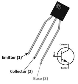
2SC1815 Transistor Pin Configuration
Pin 1 – Emitter
The emitter is the terminal through which conventional current leaves an NPN transistor. In many common-emitter circuits, the emitter is connected to ground directly or through an emitter resistor.
Pin 2 – Collector
The collector is the main current-carrying terminal. It is normally connected toward the positive supply through the load or collector resistor.
Pin 3 – Base
The base controls transistor conduction. A relatively small base current can control a larger collector current, allowing the device to function as an amplifier or electronic switch.
Features & Specifications
The features and specifications of the 2SC1815 transistor include the following.
|
Parameter |
Specification |
|
Part number |
2SC1815 |
| Transistor type |
NPN BJT |
|
Semiconductor material |
Silicon |
| Package |
TO-92 |
|
Collector-emitter voltage, VCEO |
50 V |
| Collector-base voltage, VCBO |
60 V |
|
Emitter-base voltage, VEBO |
5 V |
| Continuous collector current, IC |
150 mA |
|
Maximum base current, IB |
50 mA |
| Collector power dissipation, PC |
400 mW |
|
DC gain, hFE |
70 to 700, depending on gain class |
| Transition frequency, fT | 80 MHz minimum under specified test conditions |
| Complementary transistor |
2SA1015 |
|
Main applications |
Audio amplification, driver stages, small-signal amplification, low-current switching |
2SC1815 hFE and Gain Classification
One of the useful characteristics of the 2SC1815 is its range of DC current gain, or hFE. Different versions are classified according to their hFE range:
|
Gain class |
hFE range |
|
2SC1815-O |
70–140 |
| 2SC1815-Y |
120–240 |
|
2SC1815-GR |
200–400 |
| 2SC1815-BL |
350–700 |
These hFE values are specified under particular test conditions, typically VCE = 6 V and IC = 2 mA. They should not be interpreted as a fixed gain that the transistor will provide under every circuit condition.
For amplifier designs, the actual circuit gain depends on transistor biasing, collector and emitter resistors, signal level, temperature, load, and other circuit parameters.
2SC1815 Absolute Maximum Ratings
| Parameter |
Symbol |
Maximum rating |
|
Collector-base voltage |
VCBO | 60 V |
| Collector-emitter voltage | VCEO |
50 V |
|
Emitter-base voltage |
VEBO | 5 V |
| Collector current | IC |
150 mA |
|
Base current |
IB | 50 mA |
| Collector power dissipation | PC |
400 mW |
|
Junction temperature |
Tj | 125°C |
| Storage temperature | Tstg |
−55°C to +125°C |
How Does the 2SC1815 Work?
The 2SC1815 operates as a bipolar transistor in which the base controls the current flowing between the collector and emitter. When the transistor is properly biased in its active region, a change in base current produces a corresponding change in collector current. This characteristic makes the transistor useful for voltage and current amplification. When the transistor is driven into cutoff and saturation, it can instead operate as a switch.
The three common operating regions are:
Cutoff region
In cutoff, the transistor is essentially switched off, and collector current is very small.
Active region
In the active region, the transistor can amplify an input signal. This operating mode is commonly used in audio and small-signal amplifier circuits.
Saturation region
In saturation, the transistor is strongly turned on, and the collector-emitter voltage becomes relatively low. This region is commonly used for switching applications.
Equivalent & Complementary Transistors
A transistor should not be considered a direct replacement merely because it is another NPN transistor in a TO-92 package. Before replacing a 2SC1815, compare:
- VCEO
- VCBO
- IC
- PC
- hFE
- VCE(sat)
- fT
- Noise characteristics
- Package
- Pin configuration
- Operating temperature
- Circuit function
Potential replacement devices may include other small-signal NPN transistors, but the suitability of a specific part must be checked against the circuit requirements.
2SC1815 vs Possible Replacement Transistors
|
Parameter |
2SC1815 | 2N3904 |
BC547 |
|
Type |
NPN | NPN |
NPN |
|
Package |
TO-92 | TO-92 variants | TO-92 |
| Main use | Audio/small-signal amplification | General-purpose switching/amplification |
General-purpose amplification |
|
Pinout |
Verify from datasheet | Verify from datasheet | Verify from datasheet |
| Direct replacement? | — | Not automatically |
Not automatically |
To know how to replace it, please refer to this; Replacing Transistors in Electronic Circuits: Factors and Considerations.
The complementary PNP transistor associated with the 2SC1815 is the 2SA1015. Manufacturer documentation identifies the 2SA1015 as its complementary device.
Complementary NPN and PNP transistors are useful in push-pull amplifier and driver configurations because the two devices can perform complementary portions of the signal-processing function.
When selecting a complementary pair, compare:
- Voltage ratings
- Collector current
- hFE
- Saturation voltage
- Frequency response
- Power dissipation
- Package and pinout
2SC1815 vs 2SA1015
| Feature | 2SC1815 | 2SA1015 |
|
Transistor type |
NPN | PNP |
| Function | Amplification/driver |
Complementary amplification/driver |
|
Package |
TO-92 | TO-92 |
| Complementary relationship | — |
Complementary to 2SC1815 |
|
Typical use |
Small-signal stages |
Complementary small-signal stages |
Always check the exact manufacturer’s datasheet when designing a complementary circuit because electrical specifications and package details can vary between manufacturers.
2SC1815 as an Audio Amplifier
The 2SC1815 is particularly well suited to small-signal audio amplification. Manufacturer documentation specifically lists audio-frequency general-purpose amplifier and driver-stage applications.
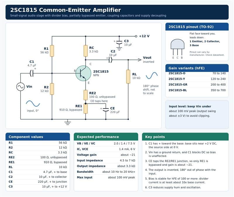
2SC1815 Common Emitter Amplifier
Before you build it, do two things. Check the 2SC1815 pinout against your datasheet, since it can vary by manufacturer. Also keep the input signal under about 100 mV peak, or the output will clip.
Common-Emitter Amplifier
A common-emitter circuit can use the 2SC1815 as the voltage-amplifying device. A typical circuit contains:
- DC supply
- Base bias resistors
- Collector resistor
- Emitter resistor
- Input coupling capacitor
- Output coupling capacitor
- Load
- 2SC1815 transistor
The exact resistor and capacitor values depend on the supply voltage, desired gain, input signal, output load, and required operating point.
For an amplifier, the transistor should be properly biased rather than simply connected as an ON/OFF switch. Proper biasing helps keep the signal within the transistor’s useful operating region and reduces distortion.
2SC1815 as a Switch
The 2SC1815 can also be used as a low-current electronic switch.
A typical switching circuit consists of:
Input signal → Base resistor → Base of 2SC1815
The load is connected in the collector circuit, while the emitter is normally connected toward ground in a common low-side switching arrangement.
The base resistor is important because it limits base current and establishes the required operating condition.
Because the 2SC1815 has a maximum collector current of 150 mA, it should not be described as a high-current load switch. Loads requiring substantially higher current are generally better controlled using a suitable power transistor or MOSFET.
How to Calculate a 2SC1815 Base Resistor?
For a simple switching circuit, the base resistor can be estimated using:
RB = (VIN − VBE) / IB
where:
RB is the base resistor.
VIN is the input voltage.
VBE is the base-emitter voltage.
IB is the desired base current.
For reliable switching, the design should also consider the required collector current and forced beta rather than assuming that the transistor will always operate at its maximum advertised hFE. This is particularly important because the hFE value varies with collector current, temperature, and individual device characteristics.
Connecting a base resistor to the base terminal of the transistor is mandatory to avoid it being damaged. Please refer to this link for; Choosing Base Resistance for Transistors in Electronic Circuits.
Advantages & Disadvantages
The advantages of the 2SC1815 NPN transistor are discussed below.
- This transistor has a high voltage tolerance feature that is very significant for some situations where high voltage is necessary. Additionally, the input & output capacitances of the transistor are fairly small, so it helps in improving the switching response & speed of the electronic circuit.
- It has outstanding high-frequency characteristics, so used in a broad range of power amplifiers & high-frequency circuit designs. Its 150MHz cutoff frequency makes it a perfect small & high-gain amplifier.
- It has low noise – 1dB & the noise voltage is only 5 microvolts, which decreases circuit interference & enhances the S/N ratio.
- These are small in size, easy to connect, flexible to use, good reliability & thermal stability, long service life, etc.
- This transistor has good compatibility and can be implemented effectively in a variety of electronic systems.
The disadvantages of the 2SC1815 NPN transistor are discussed below.
- These transistors can generate heat during working & they need additional heat-sinking systems in high-power applications.
- Due to its high voltage handling and limited power dissipation ability, this transistor is not apt for very high-power applications.
- It may not be best for audio frequency applications that need very high-speed switching or very high-frequency processes that go above its transition frequency limits.
How to Test a 2SC1815 With a Multimeter?
A digital multimeter with a diode-test function can be used for a basic transistor check.
Step 1: Identify the pins
Identify the emitter, collector, and base from the datasheet or package drawing.
For the standard 2SC1815 arrangement discussed in this article:
- Pin 1: Emitter
- Pin 2: Collector
- Pin 3: Base
Step 2: Test the base-emitter junction
Place the positive meter probe on the base and the negative probe on the emitter in diode-test mode. An NPN transistor should show a forward-biased semiconductor junction.
Reverse the probes, and the junction should normally show a much higher resistance/open-circuit indication.
Step 3: Test the base-collector junction
Repeat the same procedure between the base and collector.
Again, the junction should conduct in one direction and block in the other.
Step 4: Check the collector-emitter path
Check between collector and emitter in both directions.
A healthy transistor should not behave like a simple short circuit between these two terminals.
This test is useful for identifying a shorted or obviously damaged transistor, but it does not provide a complete test of hFE, leakage, frequency response or performance under load.
Advantages of the 2SC1815
The main advantages of the 2SC1815 include:
- NPN silicon BJT suitable for small-signal applications.
- 50 V collector-emitter voltage rating.
- 150 mA maximum collector current rating.
- Wide hFE classification from 70 to 700.
- Available in a compact TO-92 package.
- Useful for audio-frequency amplification.
- Suitable for driver-stage applications.
- Available in different gain classifications.
- Useful in low-power switching and oscillator circuits.
- Complementary 2SA1015 available for complementary amplifier designs.
2SC1815 Applications
The 2SC1815 can be used in a range of low-power electronic circuits, including:
- Audio-frequency amplifier stages
- Low-noise signal amplification
- Driver stages
- Preamplifier circuits
- Small-signal voltage amplifiers
- Low-current switching circuit
- Oscillator circuits
- Signal-conditioning circuits
- Push-pull amplifier stages
- Educational and hobby electronics projects
Its 150 mA collector-current rating means it is better suited to small-signal and low-power applications than high-power load switching.
2SC1815 in Oscillator Circuits
The transistor can also be used in oscillator and multivibrator circuits where its switching and amplification characteristics are appropriate.
For example, two NPN transistors can be configured as an astable multivibrator to generate a periodic waveform. The oscillation frequency is determined primarily by the resistor-capacitor network and transistor switching characteristics.
The circuit should be designed so that the collector current, base current, voltage and power dissipation remain within the device ratings.
2SC1815 Noise Characteristics
The 2SC1815 is often selected for low-noise signal applications. However, noise specifications must always be quoted together with their test conditions.
For example, manufacturer datasheets specify a noise figure under particular voltage, current, frequency and source-resistance conditions. Therefore, a statement such as “the transistor has 1 dB noise” should not be interpreted as a universal noise level for every circuit.
This distinction is particularly important when designing microphone preamplifiers, audio preamplifiers or other low-level signal circuits.
2SC1815 Datasheet
The datasheet is the best reference when designing a circuit around the transistor because it provides:
- Absolute maximum ratings.
- Electrical characteristics.
- hFE classification.
- Package information.
- Pin configuration.
- Saturation characteristics.
- Transition-frequency information.
- Typical characteristic curves.
Please refer to this link for the 2SC1815 NPN transistor datasheet.
Frequently Asked Questions
Is the 2SC1815 an NPN or PNP transistor?
The 2SC1815 is an NPN transistor.
What is the maximum voltage of the 2SC1815?
The maximum collector-emitter voltage rating (VCEO) is 50 V under the manufacturer’s specified conditions. The collector-base voltage rating (VCBO) is 60 V.
What is the maximum current of the 2SC1815?
The maximum continuous collector current (IC) is 150 mA.
What is the hFE of the 2SC1815?
The overall hFE range is 70 to 700, depending on the gain classification. The common classifications are O, Y, GR and BL.
What is the pinout of the 2SC1815?
For the standard TO-92 configuration described by the manufacturer, the pins are:
- Pin 1 – Emitter
- Pin 2 – Collector
- Pin 3 – Base
Always verify the package drawing for the exact manufacturer’s part.
What is the complementary transistor of the 2SC1815?
The complementary PNP transistor is the 2SA1015.
Is the 2SC1815 suitable for audio amplification?
Yes. Audio-frequency general-purpose amplifier and driver-stage applications are specifically listed for the device.
Can the 2SC1815 be used as a switch?
Yes. It can be used as a low-current switch, provided the collector current, base current, voltage, and power dissipation remain within their specified limits.
Can the 2SC1815 replace a BC547 or 2N3904?
Not automatically. The electrical ratings, hFE, switching characteristics, and especially the pinout must be compared before using one transistor as a replacement for another.
How do I identify a 2SC1815 transistor?
The device may be marked C1815 or with a manufacturer-specific marking that identifies the 2SC1815 and its gain classification. The marking should be checked against the manufacturer’s documentation.
Conclusion
The 2SC1815 is a low-power NPN silicon transistor designed primarily for small-signal amplification and driver applications. With a 50 V collector-emitter voltage rating, 150 mA collector-current rating, 400 mW collector power dissipation, and multiple hFE classifications, it is useful in audio amplifiers, preamplifiers, driver stages, oscillators, and low-current switching circuits.
Its 1-E, 2-C, 3-B pin configuration, hFE classification, maximum ratings, and complementary 2SA1015 counterpart are especially important when designing or repairing circuits.
For a replacement transistor, do not rely on the part number alone. Always compare the electrical ratings, hFE, package, pinout, and intended application with the original device’s requirements.
In short, the 2SC1815 remains a useful small-signal transistor for audio and general-purpose electronic circuits, but it should be selected within its voltage, current, power, and frequency limitations.