PNP transistor is one kind of bipolar junction transistor and it includes three terminals known as collector, emitter, and base. As compared with NPN, this transistor structure is completely different because instead of two n-type semiconductors here two p-type semiconductors are used. The separate region between these semiconductors is due to the n-type. The majority of charge carriers of this transistor are holes because two p-types of semiconductors are used in the process. The construction of both the transistors may differ but their operation and the respective characteristics remain the same. This PNP transistor is also known as the current control device. This article discusses an overview of the PNP transistor and its working.
What is a PNP Transistor?
A PNP transistor can be defined as the formation of a bipolar junction transistor can be done because of the connection established between two p-types & one n-type in the middle of it. So this is known as a PNP transistor. In this way, we can define the PNP transistor. For the applications of switching and regarding the amplification of the signals, this N-P-N transistor is preferred. The PNP transistor symbol consists of three terminals emitter, base, and collector. The arrow is sharply pointing towards the base indicating the flow of current from the emitter terminal to the base.
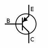
Symbol of P-N-P Transistor
PNP Transistor Construction
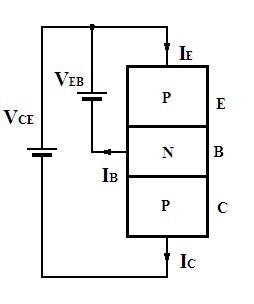
The construction of it is similar to that of the N-P-N transistor but here the differences arise in the polarities of the voltages applied. The characteristics tend to differ because here the voltage that has been applied in between the terminal base is negative and that of the emitter is positive.
The formation of the PNP transistor is due to the majority of the p-types and the one n-type in it. As the majority of charge carriers are holes here the formation of the current in this is due to the movement in the holes.
Here the junction formed because of the terminal base and the emitter is to be kept positive the reason behind this is that the holes in the terminal collector must not get into the base. The junction formed due to the terminal collector and the base is reverse biased but the base must be kept positive in comparison with the collector. Hence the holes from the collector must not enter into the base.
Hence we can conclude regarding the voltage supplies in such a way that the emitter must be supplied with the positive voltage in the comparison with the collector and the base voltages. This indicates that the biasing of the emitter must be in a positive manner with respect to that of the collector and the base.
Working
The junction formed here is because its terminals are the emitter and the base as well as the collector and the base. The junction in between the terminals of the emitter and the base is biased in forwarding conditions.
As it is in forwarding mode the majority of carriers here are the holes that get inserted into the base region. Hence the generation of the current in the emitter takes place. As the base is of n-type in this transistor the electrons are present in it. These electrons get combined with the holes entered in this region that inserted into the base.
Some of the electrons are gets combined remaining tends to move towards the collector. The reason behind this is that the base at the PNP transistor is doped with light concentration. Hence this leads to the generation of the current at the base terminal.
As the junction formed due to the terminals of collector and the base is in the reverse bias mode. The electrons entered in it get collected. Hence the generation of the current at the collector takes place.
P-N-P Transistor as Switch
In order to make the transistor work as a switch, it must be operated in certain regions. As it is already known that there are three operating regions in the bipolar junction transistors either it may be NPN or PNP.
There are three terminals emitter, base, and collector which two junctions are formed in it because the base terminal is in the middle and commonplace of interaction for emitter and collector. Based on this, the way biasing is done for the junctions the regions of the transistors are classified.
The three regions are:
- Active Region – In this one of the junctions must be kept in the forward mode of biasing and the other junction is at reverse biasing. This type of operating region in the transistor is referred to as the active region.
- Saturation Region – In this both the junctions formed due to the interaction of the terminals must be kept in forward biasing mode. This type of region is completely active for both the junctions referred to as saturation region.
- Cut-off Region – The formed junction because of the terminals must be kept in the reverse biasing mode. This indicates that no external supply is provided to any of the terminals. Hence this type of region is referred to as the cut-off region.
P-N-P Transistor Construction as a Switch
All these regions are formed in the transistors. In order to make the transistor work as a switch only two transistors are preferred either both the junctions must be completely ON that is saturation mode or the junctions must be completely OFF that is in cut-off mode. This process of operation is referred to as a switch. But the active region is not used for this purpose because the q-point in this region lies at the center.
Applications of PNP Transistor
The applications of the PNP transistor are as follows:
- These transistors are used when the outcome of the device requires a current. Therefore in this, the collector collects the current.
- The application of this type of transistor is such that it can be implemented as a switch.
- It can also be preferred during the circuits of amplification.
- During the cases of shutdowns in emergency shutdowns, the PNP transistors are preferred.
- As the pair of Darlington transistors are constructed this PNP transistor is utilized
- In order to control the flow of the current for the motors that are heavy, these transistors are useful.
- For the applications of robotics, these transistors are preferred.
Please refer to this for How to Select a Transistor.
In this way, the PNP transistor is constructed and it can be used as a switch. Now can you choose which type of BJT transistor is preferred as a Switch?