Diodes are the most frequently used electronic components in various electrical and electronic circuits. So, 1N4148 is a silicon switching signal diode registered in 1968 at JEDEC for industrial and military applications. This diode was second-sourced by various manufacturers like Texas Instruments, where its device versions are listed in October 1966. The 1N4148 diode has an enduring status within low-current applications. This diode was replaced by the older diode, such as 1N914, as cross-reference replacements for each other, thus used interchangeably. However, these diodes mainly differ in their leakage current specifications. This article provides an overview of the IN4148 Diode, pin-out, specifications, and its applications.
What is an IN4148 Diode?
The 1N4148 is the most popular & long-lived silicon switching signal diode due to its low cost and dependable specifications. This diode is available in the DO-35 package, which conducts only in the forward-biased condition. Thus, it is well known for its quick switching speeds, high conductance & and less forward voltage drop, thus helpful in applications up to 100 MHz with a 4 ns recovery time, like gate circuits of MOSFETs, IGBTs & transistors. This diode can also be utilized for changing the logic level from 5V to 3.3V.
This diode’s current-carrying capacity is up to 300mAmps which can withstand up to 2A of current. This diode has an 8ns fast recovery time at 10mAmps forward current; thus, it is appropriate wherever quick switching is necessary.
IN4148 Diode Working
The 1N4148 silicon switching signal diode works by allowing current flow from the anode terminal to the cathode. This diode includes two operating modes based on how it is coupled across the voltage source, such as forward bias & reverse bias. This diode in forward-bias mode works like a closed switch by allowing current to be supplied through it. Similarly, this diode in reverse-bias mode works as an open switch; thus, it does not allow current to flow. This switching diode exhibits higher resistance under a specified voltage, whereas it exhibits low resistance above that specific voltage.
Pin Configuration:
The pin configuration of the IN4148 diode is shown below. This diode includes two pins, which are discussed below.
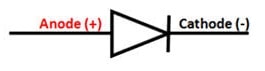
1N4148 Diode Pin Configuration
- Pin-1 (Anode): This anode pin or positive pin allows current to flow.
- Pin-2 (Cathode): Current will flow from the cathode pin or negative terminal.
Features & Specifications:
The features and specifications of the IN4148 diode include the following.
- IN4148 is a silicon switching signal diode.
- This diode is available in SMD and DO-35 packages.
- This diode is fabricated using planar technology & encapsulated within a hermetically sealed leaded glass.
- Its reverse recovery time is 8ns.
- This diode only conducts in the forward polarity condition and is a through-hole package with axial leads.
- Maximum power dissipation is 5W.
- The forward surge current maximum is 2A.
- Its RMS reverse voltage is 75 volts.
- Its maximum rectified current is 15A or 150 mA.
- The maximum reverse voltage is 100 V.
- Its maximum continuous reverse voltage is 100 Volts.
- The maximum repetitive peak reverse voltage is 100 V.
- The max repetitive peak forward current is 450 mA.
- Maximum temperature range is from -65 C to +175 Centigrade.
- The maximum continuous forward current is 300 mA.
- Its forward voltage drop is approximately 0.7 V at 10 mA forward current.
Equivalents & Alternatives
Equivalent IN4148 diodes are; 1N914, BA682 & BA684. Alternative IN4148 diodes are; IN914A, 1N914B, 1N916A, 1N916B, 1N916, 1N4448, 1N4448WS, 1N4148WS, 1N4448W.
How to Run a 1N4148 Diode in a Circuit Safely?
To use this diode for the long term within electronic circuits, it is recommended to confirm the mark on the diode’s cathode terminal. Therefore, it needs to be connected in the right polarity in the electronic circuit. According to the above-defined specifications, we should not supply high voltage and current. Thus, it is always needed to operate and store at temperatures>- 65 °C and < +175 °C.
Diodes and Transistors Tester with 555 IC
The diodes and transistors tester circuit using a 555 IC is shown below. Generally, transistors and diodes are basic components used in electronic circuits that play a major role. Whenever these components are used in any circuit, it is important to make sure that they are working properly. So, it is necessary to have a consistent technique to test diodes and transistors.
Here, we are designing very simple and efficient diode and transistor testing circuits. This circuit helps you identify whether these components are working correctly or not. Thus, this simple circuit utilizes the reliable and versatile 555 IC as a multivibrator to generate a 70 Hz frequency using resistors and a capacitor.
The required components to make this circuit mainly include: a 9V battery, resistors like 1 KΩ, 100 KΩ, 680 Ω, and 68 Ω, a 0.1 µF capacitor, 555 timer IC, D1 to D4 1N4148 diodes, 5.1 V ZD1 and ZD2 Zener diodes, LED1 and LED2 diodes, and SW1 and SW2 switches. Connect this circuit according to the diagram illustrated below.
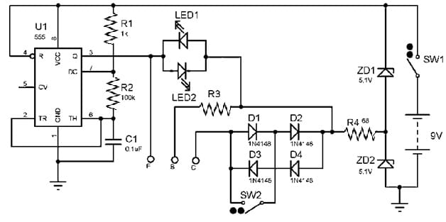
Diodes and Transistors Tester with 555 IC
Working
First, to test a transistor in this circuit, the SW2 switch must be in the off mode. In the absence of transistor testing, two LEDs in the circuit will flash. But whenever you connect an NPN or PNP transistor to the B, C & E test terminals, the voltage drop becomes lower across one of the LEDs as compared to the threshold voltage, thus causing the LED to stop glowing. This can be stated as the transistor will be in good condition. Similarly, if the two LEDs stay lit, then the transistor is said to be faulty, which has either a broken collector-emitter junction or is short-circuited.
Similarly, diode testing is very simple. When the SW2 switch is turned on, the diode under test is connected between terminals C & E. If the diode works properly, then one LED will illuminate; however, if it is defective, then both LEDs will illuminate.
One of the main benefits of this simple circuit is its simplicity. Test components like transistors & diodes are critical in electronics. The circuit is an easy & efficient method to test these components in electronic circuits to make sure that your circuits are properly working or not. This circuit is used in electronics projects to avoid time-consuming errors and costs.
Negative Voltage Generator Circuit with IN4148 Diode
A negative voltage generator circuit is shown below, which is very simple to design and needs low-cost components. Generally, negative voltage is required in electronic applications. However, having a negative supply source is not a consistent alternative whenever it is needed for low-current applications.
We cannot use a negative voltage power supply that needs low power in many electronic circuits. For low-power or reference purposes of applications, one may go for electronic circuits that can generate negative voltage using a positive voltage supply. Here, a basic negative voltage generator circuit is designed with a 555 IC.
The required components to make this circuit mainly include: a 5 to 9 V voltage supply, NE555 timer IC, 1KΩ and 10KΩ resistors, 22nF and 100nF ceramic capacitors, 22µF electrolytic capacitor, IN4148 diode, and testing probes. Connect this circuit as per the simple circuit shown below.
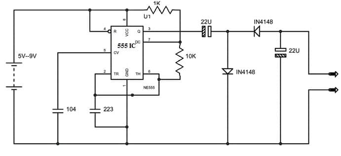
Negative Voltage Generator Circuit
Working
The above negative voltage generator circuit uses a 555 timer IC in Astable mode. Here, the capacitor in the circuit can be modified for the complete negative voltage. The 555 IC in the circuit works as a square wave generator to produce a square wave that has a positive peak & +0 a full loop.
Whenever the voltage peak at the output is positive, then there will be a current flow. The diode D1 will prefer forward at the moment, and the diode D2 will be preferred reverse. As a result, the C1 capacitor is charged, and the VCC voltage appears across it.
If the GND appears after a positive peak, then the current flow will continue. So the D1 diode is reverse-biased at the moment & the D2 diode is forward-biased. The deposited load within the capacitor C1 would have a method of flowing whenever the D2 diode fails. The C1 capacitor discharges through the D2 diode, and then the C2 capacitor is charged. Thus, a voltage in the above circuit will take place within the C2 capacitor throughout the 0 V signal.
Here, the voltage on the C2 capacitor is negative if the GND is affected. Thus, this stable charging & uploading for every loop and stable negative voltage at the output of the GND.
For several electronic circuits, we cannot utilize a negative voltage power source that requires low power. To generate a negative voltage from a positive voltage supply, one may utilize electronic circuits for referencing (or) low power-based applications.
Advantages & Disadvantages
The advantages of the IN4148 diode include the following.
- The 1N4148 diode has less than four ns recovery time, which makes it perfect for signal processing and high-frequency applications.
- It is affordable and widely available for use in electronic projects.
- These are durable and have reliable performance eventually.
- It is perfect for low-power circuits or whenever energy efficiency is a main concern.
- It is suitable mainly for small-signal applications.
- This diode has a relatively low power loss throughout conduction, so it is significant in the efficient utilization of electricity within electronic circuits.
- It is stable in various operating conditions; thus, it is simple to use & does not need special operating conditions.
- These diodes have high resistance at a fixed voltage, while they have less resistance over a fixed voltage.
The disadvantages of the IN4148 diode include the following.
- The 1N4148 diode has a somewhat low surge current rating.
- It has 4pF maximum intrinsic capacitance; thus, it can be a design parameter to consider for higher-frequency circuits.
- This diode enters the breakdown zone whenever 100 volts are provided to the two terminals in the reverse direction.
- It has a somewhat low surge current rating.
- This diode has a low conduction voltage & transmission current.
- It has a slightly slower switching speed.
- Intermittent opens can happen if the soldering of the diode doesn’t wet the terminal frame.
- The backside metallization of the cathode can peel off within layers.
IN4148 Diode Applications
The applications of the IN4148 diode include the following.
- IN4148 diode is used in voltage regulation, protection circuits, and signal processing.
- This diode is ideal for applications that need quick response times, like digital circuits.
- It is used commonly in RF (radio frequency) applications for demodulating signals.
- This diode is used in MOSFETs, IGBTs, and gate circuits of transistors for quick signal transfer from the integrated circuit.
- It is used with high signal frequency in different circuits.
- The applications of this diode involve different circuits like Communications, TV circuits, industrial control circuits & computers.
Please refer to this link for the IN4148 Diode Datasheet.
Thus, this is an overview of the IN4148 diode, including its pin configuration, features, specifications, circuit, operation, pros, cons, and applications. The 1N4148 is a normal silicon diode that is very famous because of its low cost, reliability & dependable specifications. It is a high-frequency and small-signal diode that is utilized for one-way conduction isolation. This diode is used in the gate circuits of MOSFETs, IGBTs & transistors to enable fast signal transmission from the chip. Here is a question for you: what is a 1N914 diode?