STM32F103 is a family of 32-bit microcontrollers developed by STMicroelectronics and based on the Arm Cortex-M3 processor core. These microcontrollers are designed for embedded applications that require good processing performance, a wide range of peripherals, low-power operating modes, and flexible communication interfaces.
The STM32F103 family belongs to the STM32F1 series and includes several devices with different Flash memory sizes, SRAM capacities, package options, GPIO counts, and peripheral configurations. Depending on the particular device, features can include 12-bit ADCs, timers, PWM, USART, SPI, I²C, CAN, USB, DMA, RTC, and other peripherals.
Because of this combination of processing capability and peripheral support, STM32F103 devices have been widely used in industrial control, motor control, consumer electronics, measurement systems, robotics, communication equipment, and many other embedded applications.
This article provides an overview of the STM32F103 family, including its features, pin configuration, architecture, memory system, clock sources, communication interfaces, boot modes, power supply, LED interfacing, and applications.
What is the STM32F103 Microcontroller?
The STM32F103 is a 32-bit RISC-based microcontroller family built around the Arm Cortex-M3 processor core. Depending on the device, the maximum CPU frequency can reach 72 MHz.
The family operates from a low-voltage power supply and combines a processor core with Flash memory, SRAM, timers, GPIOs, analog peripherals, communication interfaces, interrupt controllers, and other system resources on a single chip.
Keep in mind that STM32F103 is a family name, not a single device. Therefore, the exact memory size, number of GPIO pins, timers, ADC channels, communication interfaces, and package type depend on the specific part number.
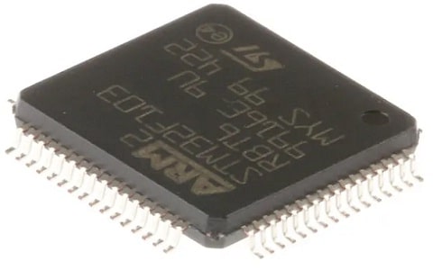
STM32F103 Microcontroller
STM32F103 devices are available in different Flash-memory configurations, ranging from lower-capacity devices to higher-density variants. They are also offered in several package options, allowing designers to select a device according to the required number of I/O pins and peripheral resources.
The processor core provides features such as:
- 32-bit Arm Cortex-M3 architecture
- Maximum CPU frequency of up to 72 MHz, depending on the device
- Nested Vectored Interrupt Controller (NVIC)
- Hardware multiplication and division
- 24-bit SysTick timer
- Multiple low-power operating modes
- DMA support
- Flexible clock system
- Integrated Flash memory and SRAM
The STM32F103 family is particularly popular in embedded systems because it provides considerably more processing and peripheral capability than many traditional 8-bit and 16-bit microcontrollers while remaining suitable for cost-sensitive designs.
STM32F103 Features and Specifications
The exact specifications vary between STM32F103 devices. The following list summarizes the major features available across the family.
- 32-bit Arm Cortex-M3 processor core
- CPU frequency of up to 72 MHz on applicable devices
- Flash memory and SRAM capacities that vary according to the device
- 12-bit analog-to-digital converters
- General-purpose and advanced-control timers
- PWM generation
- DMA controllers
- Nested Vectored Interrupt Controller (NVIC)
- External interrupt/event controller
- GPIO ports with configurable input and output functions
- USART interfaces
- SPI interfaces
- I²C interfaces
- CAN interface on applicable devices
- USB Full-Speed interface on applicable devices
- Independent and window watchdog timers
- Internal high-speed and low-speed RC oscillators
- External high-speed and low-speed clock inputs
- PLL-based clock generation
- Sleep, Stop, and Standby low-power modes
- Factory-trimmed internal oscillators
- Unique device identification on applicable devices
- Multiple package configurations
Important Note About STM32F103 Specifications
Since the STM32F103 family contains multiple device variants, specifications should always be checked against the exact part number before selecting a device for a hardware design.
For example, a high-density STM32F103 device can provide more memory and peripherals than a lower-density member of the family. Therefore, features such as the number of USARTs, SPI interfaces, ADC channels, timers, Flash memory, SRAM, and available GPIOs should not be assumed to be identical across all STM32F103 devices.
STM32F103 Pin Configuration
STM32F103 devices are available in different packages, so the number and arrangement of pins depend on the particular device and package.
A typical STM32F103 device provides GPIO ports such as Port A, Port B, and Port C, along with power, reset, oscillator, and boot-configuration pins. Higher-pin-count variants can provide additional GPIO ports and peripheral functions.
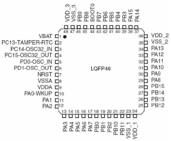
STM32F103 Microcontroller Pin Configuration
VDD and VSS:
VDD pins provide the digital supply voltage, while VSS pins are connected to ground.
VDDA and VSSA:
These pins provide the analog supply and ground connections for analog circuitry such as the ADC and other analog functions. Proper decoupling and grounding are important when using the analog peripherals.
VBAT:
The VBAT pin supplies the backup domain when the main VDD supply is unavailable. It can be used to maintain functions such as the RTC and backup registers, depending on the device configuration.
NRST:
NRST is the external reset input. Pulling this pin to the active reset level resets the microcontroller.
OSC_IN and OSC_OUT:
These pins are used with an external high-speed crystal or oscillator when an external clock source is required.
PC14-OSC32_IN and PC15-OSC32_OUT:
These pins are associated with the low-speed external oscillator, commonly used with a 32.768 kHz crystal for RTC applications.
BOOT0:
BOOT0 is used together with the device’s boot configuration to select the memory area from which the microcontroller starts execution.
GPIO pins:
GPIO pins can be configured for digital input, digital output, alternate functions, or analog operation, depending on the pin and device.
Because alternate functions are assigned to specific pins, the datasheet and reference manual for the exact STM32F103 part should always be consulted when designing a circuit.
STM32F103 Microcontroller Architecture
The STM32F103 architecture combines the Cortex-M3 processor core with memory, buses, DMA, timers, communication peripherals, analog peripherals, GPIO, clock circuitry, and interrupt controllers.
The main architectural blocks are described below.
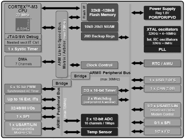
STM32F103 Microcontroller Architecture
Arm Cortex-M3 Core
The Cortex-M3 is the processing core of the STM32F103. It is a 32-bit RISC processor designed specifically for embedded applications.
The core provides efficient instruction execution, hardware multiplication and division, interrupt handling through the NVIC, and support for low-power operation.
For STM32F103 devices operating at up to 72 MHz, the Cortex-M3 provides sufficient processing performance for applications such as motor control, industrial automation, communication systems, and embedded instrumentation.
Bus Architecture
The Cortex-M3 uses separate paths for instruction and data access. The STM32F103 also contains an internal bus architecture that connects the processor and DMA controllers to memory and peripheral resources.
The major buses include:
- I-Code bus: Used primarily for instruction access from Flash memory.
- D-Code bus: Used for data access associated with the Flash memory interface.
- System bus: Provides access between the processor and system resources.
- AHB: The Advanced High-performance Bus connects high-speed system resources.
- APB1 and APB2: Advanced Peripheral Buses connect the peripheral blocks.
The APB1 and APB2 peripheral clocks can operate at different frequencies, depending on the selected system-clock configuration.
Memory System
The STM32F103 contains two primary types of internal memory:
Flash memory:
Flash memory stores the application program and other non-volatile information. The available Flash capacity depends on the specific STM32F103 device.
SRAM:
SRAM is used for temporary data during program execution, including variables, stack memory, and buffers. Its capacity also varies according to the device. The exact memory organization should be checked in the datasheet for the selected part number.
Nested Vectored Interrupt Controller (NVIC)
The Nested Vectored Interrupt Controller, or NVIC, is part of the Cortex-M3 processor core. It manages interrupts generated by the processor and peripherals.
Interrupts allow the microcontroller to respond to events without continuously checking every peripheral in software. The NVIC also supports configurable interrupt priorities, allowing more important events to be handled before lower-priority interrupts.
External Interrupt/Event Controller (EXTI)
- The External Interrupt/Event Controller allows selected GPIO signals and other sources to generate interrupts or events.
- An external device such as a push button, sensor, or digital signal source can therefore trigger software execution when a specified signal transition occurs.
- The exact number of EXTI lines and their mapping depends on the device.
STM32F103 Clock System
The clock system determines the operating frequency of the processor and peripherals. STM32F103 devices provide several internal and external clock sources.
The main clock sources include:
High-Speed Internal Oscillator (HSI)
HSI is an internal RC oscillator with a nominal frequency of 8 MHz. It can be used as a system-clock source without requiring an external crystal.
High-Speed External Oscillator (HSE)
HSE uses an external crystal, ceramic resonator, or external clock source. It is useful when a more accurate or application-specific clock frequency is required.
Phase-Locked Loop (PLL)
The PLL multiplies a selected clock source to produce a higher-frequency system clock. With the appropriate configuration, STM32F103 devices can operate at frequencies up to 72 MHz.
Low-Speed Internal Oscillator (LSI)
LSI is a low-frequency internal RC oscillator. It can be used for low-speed clocking and watchdog-related functions.
Low-Speed External Oscillator (LSE)
LSE is an external low-speed oscillator, commonly implemented using a 32.768 kHz crystal. It is primarily used for accurate RTC operation.
System Clock
After reset, the microcontroller starts with a default clock configuration. The application can then configure the clock tree to select HSI, HSE, or PLL as the system clock source.
The selected clock configuration also determines the frequencies supplied to the AHB, APB1, and APB2 buses and their associated peripherals.
Boot Modes
Boot mode determines the memory source from which the STM32F103 starts executing after reset.
The main boot sources are:
- Main Flash memory
- System memory
- Embedded SRAM
The boot configuration pins determine the selected boot mode. System memory contains the factory-programmed bootloader on supported devices, which can be used for programming the device through supported interfaces.
The exact boot configuration should be checked in the reference manual and datasheet for the selected STM32F103 device.
Power Supply
A stable power supply is essential for reliable microcontroller operation.
VDD
VDD provides the main digital supply voltage for the microcontroller and its I/O circuitry. STM32F103 devices are designed for low-voltage operation, with the exact operating range specified in the corresponding datasheet.
VDDA
VDDA supplies the analog circuitry. When using ADCs or other analog functions, VDDA should be connected and decoupled according to the manufacturer’s recommendations.
VSSA
VSSA provides the analog ground connection.
VBAT
VBAT powers the backup domain when the main supply is unavailable. This domain can maintain RTC and backup-register functions.
POR, PDR, and PVD
The STM32F103 includes power monitoring and reset circuitry.
- POR (Power-On Reset) helps ensure proper startup when power is applied.
- PDR (Power-Down Reset) helps maintain the MCU in reset when the supply voltage is too low for reliable operation.
- PVD (Programmable Voltage Detector) monitors VDD against a programmable threshold and can generate an interrupt when the supply voltage crosses the selected level.
DMA Controller
- DMA stands for Direct Memory Access.
- DMA allows data to be transferred between memory and peripherals without requiring the CPU to handle every individual data transfer.
- For example, DMA can be used to transfer ADC conversion results into memory or move data between memory and communication peripherals.
- This reduces CPU overhead and can improve the efficiency of applications that handle continuous data streams.
- The number of DMA controllers and channels depends on the specific STM32F103 variant.
Timers
Timers are among the most useful peripherals in STM32F103 devices. They can be used for:
- Time measurement
- Periodic interrupts
- PWM generation
- Input capture
- Output compare
- Pulse measurement
- Motor-control applications
- Encoder interfaces
Many STM32F103 variants provide several 16-bit timers, although the exact number and capabilities depend on the device.
General-Purpose Timers
General-purpose timers contain counters, prescalers, and capture/compare channels. They can generate interrupts and PWM signals or measure external signals.
Advanced-Control Timer
The advanced-control timer provides features intended for applications such as motor control. These can include complementary PWM outputs, dead-time insertion, and emergency shutdown functions.
I²C Interface
I²C, or Inter-Integrated Circuit, is a two-wire serial communication interface.
It uses:
- SCL — Serial Clock
- SDA — Serial Data
The interface supports communication between a controller and multiple connected devices using device addresses.
I²C is commonly used to connect sensors, EEPROMs, RTC modules, displays, and other peripheral devices.
STM32F103 devices provide I²C interfaces, with the exact number depending on the variant.
USART Interface
USART stands for Universal Synchronous/Asynchronous Receiver/Transmitter.
It is commonly used for serial communication between the microcontroller and external devices such as:
- PCs
- GPS modules
- Bluetooth modules
- GSM modules
- Other microcontrollers
- Industrial equipment
USART can operate in asynchronous mode, which is commonly used for UART-style serial communication, or in synchronous modes where supported.
The number of USART interfaces and their available features depend on the STM32F103 device.
SPI Interface
SPI, or Serial Peripheral Interface, is a synchronous serial communication protocol.
A typical SPI connection uses:
- SCK — Serial clock
- MOSI — Master Out, Slave In
- MISO — Master In, Slave Out
- NSS/CS — Chip-select signal
SPI is useful when high-speed communication is required with devices such as displays, memory chips, sensors, and converters.
The available SPI interfaces and maximum clock rates depend on the selected STM32F103 variant and clock configuration.
CAN Interface
CAN stands for Controller Area Network. It is a robust communication protocol widely used in automotive and industrial applications.
CAN allows multiple controllers and devices to communicate over a shared bus without requiring a central host.
STM32F103 devices that include CAN can support applications such as:
- Automotive control systems
- Industrial controllers
- Motor-control networks
- Distributed embedded systems
The exact CAN capabilities should be checked for the selected device.
USB Interface
- Some STM32F103 devices include a USB 2.0 Full-Speed interface.
- USB can be used to communicate with computers and other USB hosts or devices, depending on the capabilities of the specific STM32F103 variant and the application design.
- USB Full-Speed provides a signaling rate of 12 Mbit/s.
- The STM32F103 should not be described as supporting USB High-Speed or SuperSpeed simply because those USB standards exist. The applicable USB capability depends on the MCU hardware.
GPIO
It stands for General-Purpose Input/Output. GPIO pins allow the microcontroller to interact with external hardware. A pin can be configured as a digital input to read a signal or as a digital output to control an external device.
GPIOs can also provide alternate functions for peripherals such as:
- Timers
- USART
- SPI
- I²C
- CAN
- USB
- Other device-specific functions
The number of available GPIO pins depends on the STM32F103 device and package.
ADC
- ADC stands for Analog-to-Digital Converter.
- An ADC converts an analog voltage into a digital value that can be processed by the microcontroller.
- STM32F103 devices provide 12-bit ADCs. These can be used with sensors, potentiometers, battery-monitoring circuits, and other analog signals.
- The number of ADC units and available input channels varies among STM32F103 devices.
RTC and Backup Registers
The Real-Time Clock (RTC) provides timekeeping functionality and can continue operating from the backup domain when the main power supply is unavailable, provided an appropriate backup source is available.
The RTC can be used for:
- Timekeeping
- Date and calendar functions
- Periodic events
- Alarm functions
Backup registers provide a small area for retaining information across certain reset or power conditions.
Low-Power Modes
STM32F103 devices provide several power-saving modes, including:
- Sleep mode
- Stop mode
- Standby mode
These modes allow developers to reduce power consumption when the processor or peripherals do not need to operate continuously.
The choice of mode depends on the application requirements and the peripherals that need to remain active.
STM32F103 LED Interfacing
One of the simplest ways to understand GPIO operation is to connect an LED and a push button to the microcontroller.
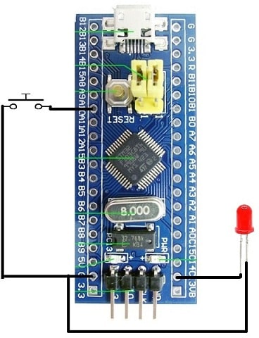
STM32F103 Microcontroller Interfacing with LED
In this example:
- One GPIO pin is configured as an output to control the LED.
- Another GPIO pin is configured as an input to read the push button.
- The button uses a pull-up configuration.
- Pressing the button changes the input state.
- The software detects the button state and controls the LED accordingly.
A current-limiting resistor must be connected in series with the LED to limit the current flowing through the LED and GPIO.
For a simple external LED circuit, the connection can be arranged as follows:
- Connect a GPIO output pin to the LED through a suitable current-limiting resistor.
- Connect the other side of the LED to the appropriate supply or ground, depending on whether the circuit is active-high or active-low.
- Connect the push button between the selected GPIO input and ground.
- Enable the GPIO’s internal pull-up resistor, or use an external pull-up resistor.
The exact GPIO pins can be changed according to the selected STM32F103 device and circuit design.
STM32F103 Clock Configuration for the Example
STM32F103 devices can use the internal HSI oscillator or an external HSE oscillator as the clock source.
For applications that require the maximum 72 MHz system frequency, the PLL must be configured correctly. A simple example can also use the 8 MHz HSI directly if high clock speed is not required.
It is important that the clock explanation and the actual program configuration match. If the program selects HSI directly as SYSCLK, the MCU is not running at 72 MHz unless the clock tree is configured accordingly.
STM32F103 LED and Push-Button Program using HAL
The following example demonstrates the basic GPIO operation using the STM32 HAL library.
The program initializes the HAL, configures the system clock, and initializes the GPIO pins. It then continuously checks the push-button state and changes the LED output accordingly.
#include “main.h”
void SystemClock_Config(void);
static void MX_GPIO_Init(void);
int main(void)
{
HAL_Init();
SystemClock_Config();
MX_GPIO_Init();
while (1)
{
if (HAL_GPIO_ReadPin(Ibutton_GPIO_Port, Ibutton_Pin) == GPIO_PIN_RESET)
{
/* Button pressed */
HAL_GPIO_WritePin(Led_GPIO_Port,
Led_Pin,
GPIO_PIN_SET);
}
else
{
/* Button released */
HAL_GPIO_WritePin(Led_GPIO_Port,
Led_Pin,
GPIO_PIN_RESET);
}
}
}
In this example, HAL_GPIO_ReadPin() reads the state of the push-button input, while HAL_GPIO_WritePin() controls the LED output.
The symbols GPIO_PIN_SET and GPIO_PIN_RESET are used to set the GPIO output to the corresponding logic state.
The exact LED logic depends on how the LED is connected. If the LED is active-low, the SET and RESET states need to be reversed.
GPIO Initialization
A typical GPIO initialization routine enables the required GPIO clocks and configures one pin as an output and another as an input with a pull-up resistor.
static void MX_GPIO_Init(void)
{
GPIO_InitTypeDef GPIO_InitStruct = {0};
/* Enable GPIO clocks */
__HAL_RCC_GPIOA_CLK_ENABLE();
__HAL_RCC_GPIOC_CLK_ENABLE();
/* Configure LED pin */
HAL_GPIO_WritePin(Led_GPIO_Port,
Led_Pin,
GPIO_PIN_RESET);
GPIO_InitStruct.Pin = Led_Pin;
GPIO_InitStruct.Mode = GPIO_MODE_OUTPUT_PP;
GPIO_InitStruct.Pull = GPIO_NOPULL;
GPIO_InitStruct.Speed = GPIO_SPEED_FREQ_LOW;
HAL_GPIO_Init(Led_GPIO_Port, &GPIO_InitStruct);
/* Configure push-button pin */
GPIO_InitStruct.Pin = Ibutton_Pin;
GPIO_InitStruct.Mode = GPIO_MODE_INPUT;
GPIO_InitStruct.Pull = GPIO_PULLUP;
HAL_GPIO_Init(Ibutton_GPIO_Port, &GPIO_InitStruct);
}
The actual pin definitions and GPIO-port clocks should be generated or configured according to the selected STM32F103 device and development board.
How the Program Works?
After initialization, the microcontroller enters the while (1) loop.
The program continuously reads the push-button input:
- The button is configured with a pull-up resistor.
- When the button is not pressed, the input remains at a logic-high level.
- Pressing the button connects the input to ground, producing a logic-low level.
- The program detects this low level.
- The LED output is changed accordingly.
This simple example demonstrates the basic GPIO operations required in many embedded applications.
For a real push-button application, software debouncing may also be required to prevent multiple transitions caused by mechanical contact bounce.
STM32F103 Applications
The STM32F103 family can be used in a wide range of embedded applications because of its processing capability, timers, ADCs, communication interfaces, GPIOs, and low-power modes.
Common applications include:
- Industrial automation
- Motor-control systems
- Robotics
- Embedded control systems
- Measurement and instrumentation
- Consumer electronics
- GPS and navigation equipment
- Printers and scanners
- HVAC controllers
- Alarm systems
- Power electronics
- Inverters
- Handheld equipment
- Medical and laboratory equipment
- Communication equipment
- Gaming and PC peripherals
- Automotive auxiliary control systems
- Data acquisition systems
The suitability of a particular STM32F103 device depends on the memory requirements, number of GPIOs, communication interfaces, ADC channels, timers, package, and other features required by the application.
Advantages of STM32F103
The STM32F103 family offers several advantages for embedded-system development:
- 32-bit Cortex-M3 processing
- Clock speeds of up to 72 MHz on applicable devices
- Wide range of integrated peripherals
- Multiple communication interfaces
- 12-bit ADC capability
- Flexible timer and PWM resources
- DMA support
- Multiple power-saving modes
- Several package and memory options
- Large ecosystem of development tools and software libraries
- Suitable for both learning and commercial embedded applications
Things to Consider When Selecting an STM32F103
Because STM32F103 is a family rather than a single device, the part number should be selected according to the application.
Before designing a circuit, check:
- Flash memory capacity
- SRAM capacity
- Number of GPIO pins
- Package type
- ADC channels
- Timer availability
- USART interfaces
- SPI interfaces
- I²C interfaces
- CAN availability
- USB availability
- Operating voltage
- Operating temperature range
- Available alternate-function pins
The datasheet and reference manual for the exact part number should be used as the final reference during hardware and software development.
STM32F103 Datasheet
For detailed electrical specifications, memory organization, pin assignments, peripheral information, and operating conditions, refer to the official STM32F103 documentation from STMicroelectronics.
[STM32F103 Datasheet – STMicroelectronics]
Conclusion
The STM32F103 is a versatile 32-bit microcontroller family based on the Arm Cortex-M3 processor. Its combination of processing performance, memory, GPIOs, timers, ADCs, communication interfaces, DMA, interrupt support, and low-power modes makes it suitable for a wide range of embedded applications.
One of the main strengths of the STM32F103 family is its flexibility. Developers can choose from different devices and package options depending on the required memory, number of I/O pins, communication interfaces, timers, and other peripherals. This makes the family suitable for both relatively simple control applications and more complex embedded systems.
The STM32F103 is also a popular choice for learning embedded programming because it provides access to many important microcontroller concepts, including GPIO control, timers, interrupts, ADCs, PWM, serial communication, clock configuration, and low-power operation.
However, STM32F103 should not be treated as a single fixed specification. Features such as Flash memory, SRAM, GPIO count, ADC channels, timers, USB, CAN, and communication interfaces vary between devices. Therefore, the datasheet and reference manual for the exact part number should always be consulted before designing hardware or writing application software.
Overall, the STM32F103 remains a capable and practical microcontroller family for embedded development, especially in applications where a 32-bit processor and a broad set of integrated peripherals are required.
Frequently Asked Questions About STM32F103
1. What is STM32F103?
STM32F103 is a family of 32-bit microcontrollers from STMicroelectronics. These devices are based on the Arm Cortex-M3 processor and are designed for embedded applications involving control, communication, sensing, and data processing.
2. Is STM32F103 a 32-bit microcontroller?
Yes. STM32F103 devices use the 32-bit Arm Cortex-M3 processor core. The processor is designed for efficient embedded-system operation and supports a range of hardware and software features intended for real-time applications.
3. What is the maximum clock frequency of STM32F103?
The maximum CPU frequency is up to 72 MHz for applicable STM32F103 devices. The actual operating frequency depends on the clock source, PLL configuration, voltage conditions, and the specific device.
4. How much Flash memory does STM32F103 have?
The Flash memory capacity varies between STM32F103 devices. Different variants are available with different memory sizes, so the exact Flash capacity should be checked using the part number and its datasheet.
For example, the commonly used STM32F103C8 device has a different memory configuration from higher-density STM32F103 variants.
5. How much SRAM is available in STM32F103?
SRAM capacity also varies across the STM32F103 family. SRAM is used for runtime data such as variables, stack memory, buffers, and other temporary information.
The exact SRAM size should be verified from the datasheet of the selected device.
6. Does STM32F103 have an ADC?
Yes. STM32F103 devices include 12-bit ADCs. They can convert analog input voltages into digital values that the processor can use.
ADC peripherals are commonly used for reading sensors, potentiometers, battery voltages, temperature signals, and other analog sources.
7. Does STM32F103 have a DAC?
The STM32F103 performance-line devices generally do not include an integrated DAC. When a true analog voltage output is required, an external DAC or another suitable circuit may be needed.
PWM can also be filtered to produce an analog-like voltage in applications where the accuracy and bandwidth requirements permit it.
8. Does STM32F103 support PWM?
Yes. PWM can be generated using the microcontroller’s timer peripherals.
PWM is commonly used for:
- Motor-speed control
- LED brightness control
- Servo control
- Power-control applications
- Signal generation
The number of PWM channels and their available pins depend on the specific STM32F103 variant.
9. What communication interfaces are available in STM32F103?
Depending on the device, STM32F103 can provide interfaces such as:
- USART/UART
- SPI
- I²C
- CAN
- USB
Not every STM32F103 device contains all of these interfaces, so the exact part number should be checked before selecting it for a communication-based application.
10. Does STM32F103 support USB?
Some STM32F103 devices include a USB Full-Speed device interface. USB Full-Speed operates at a signaling rate of 12 Mbit/s.
USB availability depends on the specific STM32F103 variant and package.
11. Does STM32F103 support CAN communication?
Yes, CAN is available on applicable STM32F103 devices. CAN is particularly useful for automotive, industrial, motor-control, and other distributed-control applications.
However, CAN availability is device-dependent and should be confirmed in the datasheet.
12. What programming languages can be used with STM32F103?
STM32F103 can be programmed primarily using C and C++. C is particularly common in embedded development because it provides efficient access to hardware resources while remaining relatively portable.
Development can be done using tools and libraries such as STM32CubeIDE, STM32CubeMX, the STM32 HAL library, CMSIS, or other compatible toolchains.
13. How is STM32F103 programmed?
- STM32F103 devices can commonly be programmed and debugged through the SWD (Serial Wire Debug) interface using a compatible ST-LINK debugger/programmer.
- Some devices also contain a factory-programmed system bootloader that can support programming through supported interfaces such as USART.
- The available programming method depends on the device, board design, and boot configuration.
14. What is the difference between STM32F103 and STM32F103C8T6?
- STM32F103 refers to the family, while STM32F103C8T6 identifies a particular device and package variant.
- The letters and numbers in the part number identify characteristics such as the device series, pin count/package, memory density, and other ordering information.
- Therefore, it is important to distinguish between the general STM32F103 family and a specific part such as STM32F103C8T6.
15. Can STM32F103 be used for motor control?
Yes. STM32F103 devices can be used for various motor-control applications because they provide timers, PWM outputs, ADCs, interrupts, and other peripherals.
The exact suitability depends on the motor type, control algorithm, required PWM channels, feedback signals, and other application requirements.
16. Does STM32F103 support low-power operation?
Yes. STM32F103 devices provide several low-power modes, including Sleep, Stop, and Standby modes.
These modes allow developers to reduce power consumption when the processor or certain peripherals do not need to operate continuously.
17. What is the difference between STM32F103 and Arduino-based microcontrollers?
STM32F103 and Arduino are not directly comparable categories. STM32F103 is a microcontroller family, whereas Arduino is a hardware/software development ecosystem.
An STM32F103-based board can provide significantly more flexibility for low-level embedded development, while Arduino platforms are often designed to make development easier for beginners through simplified libraries and development tools.
STM32F103 can also be programmed using Arduino-compatible environments on supported boards, although professional STM32 development typically uses tools such as STM32CubeIDE and the STM32 software ecosystem.
18. Is STM32F103 suitable for beginners?
Yes. STM32F103 is a good platform for learning embedded-system concepts once the developer is comfortable with basic C programming.
It can be used to learn:
- GPIO programming
- Timers
- Interrupts
- PWM
- ADC
- UART/USART
- SPI
- I²C
- DMA
- Clock configuration
- Embedded debugging
Development boards based on STM32F103 can make it easier to experiment with these peripherals before designing a custom PCB.
19. What should be checked before selecting an STM32F103 device?
Before choosing a particular STM32F103 device, check the following:
- Flash memory size
- SRAM size
- GPIO count
- Package type
- ADC channels
- Timer resources
- PWM channels
- USART/UART interfaces
- SPI interfaces
- I²C interfaces
- CAN availability
- USB availability
- Operating voltage
- Operating temperature range
- Required alternate-function pins
- Development and programming requirements
The exact part number should always be checked against the latest device documentation before starting a hardware design.