The BF199 transistor is a high-frequency NPN bipolar junction transistor (BJT) primarily designed for radio frequency (RF) amplification, intermediate frequency (IF) amplification, and signal-processing applications. It is commonly used in radio receivers, television circuits, FM transmitters, RF amplifiers, oscillators, and various electronic projects.
Manufacturers may offer BF199 transistors with slightly different electrical characteristics, including transition frequency, collector current, power dissipation, and voltage ratings. For example, published specifications may indicate different transition frequencies depending on the manufacturer and device variant. Therefore, consult the datasheet from the actual manufacturer before selecting or replacing this transistor.
This article explains the BF199 transistor pinout, working principle, features, electrical specifications, equivalent transistors, safe operating conditions, practical circuit applications, advantages, disadvantages, and testing methods.
What is the BF199 Transistor?
The BF199 is an NPN silicon bipolar junction transistor designed primarily for high-frequency signal amplification. It is well-suited for RF amplifiers, video intermediate-frequency (IF) amplifiers, radio receivers, and other circuits that require high-frequency signal processing.
Like other bipolar junction transistors, the BF199 consists of three semiconductor regions: the emitter, base, and collector. These regions form two PN junctions that control the flow of electrical current through the device.
The three terminals perform the following functions:
- Emitter: Supplies charge carriers into the transistor.
- Base: Controls the current flowing through the transistor.
- Collector: Collects charge carriers and delivers the output current.
The BF199 operates by using a small base current to control a larger collector-to-emitter current. When a suitable bias voltage is applied, the transistor can operate in its active region to amplify electrical signals. It can also operate in cutoff and saturation regions for switching applications.
One of the main characteristics of the BF199 is its high transition frequency, which makes it suitable for applications where ordinary low-frequency transistors may not provide adequate performance.
Before selecting this transistor for a particular circuit, consider its voltage ratings, collector current, power dissipation, gain, frequency response, and package configuration. For additional guidance, refer to How to Select a Transistor.
While looking for a suitable transistor for your application based on a few factors, it is very important to look into a few points on How to Select a Transistor.
BF199 Transistor Pin Configuration
The BF199 transistor has three terminals: collector, emitter, and base. These terminals allow the transistor to connect to an external electronic circuit. The following diagram illustrates the BF199 transistor pin configuration.
The three terminals are described below.
- Pin 1 – Collector (C): The collector terminal collects charge carriers from the base-emitter region and provides the output current to the connected circuit.
- Pin 2 – Emitter (E): The emitter terminal supplies charge carriers into the transistor’s base region.
- Pin 3 – Base (B): The base terminal controls the collector current by regulating the transistor’s operation.
Note: Always verify the pin arrangement using the datasheet of the specific manufacturer and package. The viewing direction of the transistor drawing is important when identifying its terminals.
Features & Specifications:
The BF199 transistor offers several characteristics that make it suitable for RF and IF amplification circuits. Its compact package, relatively low capacitance, and high-frequency performance are useful in many electronic designs.
The important features include:
- Transistor type: NPN bipolar junction transistor.
- Semiconductor material: Silicon (Si).
- Mounting type: Through-hole.
- Package type: TO-92 (manufacturer-dependent).
- Maximum collector power dissipation (Pc): 0.25 W.
- Maximum collector-base voltage (VCBO): 40 V.
- Maximum collector-emitter voltage (VCEO): 20 V.
- Maximum emitter-base voltage (VEBO): 4 V.
- Maximum collector current (IC): 25 mA.
- Maximum junction temperature (Tj): 125°C.
- Transition frequency (fT): 275 MHz.
- Collector capacitance (Cc): 0.6 pF.
- Minimum DC gain (hFE): 38.
- Storage and operating temperature limits: Check the specific manufacturer’s datasheet.
BF199 Transistor Electrical Specifications
The following table summarizes the commonly referenced electrical characteristics of the BF199 transistor.
|
Parameter |
Specification |
|
Transistor type |
NPN |
|
Material |
Silicon |
| Package |
TO-92 |
|
Collector power dissipation |
250 mW |
| Collector-base voltage |
40 V |
|
Collector-emitter voltage |
20 V |
| Emitter-base voltage |
4 V |
|
Maximum collector current |
25 mA |
|
Transition frequency |
275 MHz |
| Collector capacitance |
0.6 pF |
|
Minimum DC gain |
38 |
| Maximum junction temperature |
125°C |
BF199 Equivalent Transistors and Replacements
Several transistors have electrical characteristics that may make them suitable alternatives to the BF199 in certain electronic circuits.
Some commonly referenced BF199 equivalents and related transistor types include:
- BF197
- BF198
- BF200
- BF202
- BF203
- BF206
- BF207
- BF208
- BF209
- BC639
- 2N9018
- C3355
However, these transistors should not automatically be considered direct replacements. Their voltage ratings, current gain, transition frequency, collector current, power dissipation, and pin configurations may differ.
Before replacing a BF199 transistor, compare the electrical characteristics of both devices and verify that the replacement is suitable for the intended application.
Replacing a suitable transistor in any circuit based on requirements is very important. To know how to replace it, please refer to this: Replacing Transistors in Electronic Circuits: Factors and Considerations.
How to Select a Suitable BF199 Replacement?
Consider the following parameters when selecting an alternative:
- Collector-emitter voltage: The replacement must support the maximum voltage present in the circuit.
- Collector current: Its current rating must be sufficient for the connected load.
- Power dissipation: Verify that the replacement can safely dissipate the generated heat.
- Current gain: Select a transistor with a suitable hFE value for the required amplification.
- Transition frequency: The replacement should provide sufficient frequency response for the RF or IF application.
- Pin configuration: Check the collector, base, and emitter arrangement before installation.
- Package type: Ensure that the replacement can be physically mounted and adequately cooled.
How to Use the BF199 Transistor Safely in a Circuit?
Proper operating conditions are important for maintaining the performance and reliability of the BF199 transistor.
For improved reliability, avoid operating the transistor continuously at its absolute maximum electrical ratings. A practical approach is to maintain a suitable safety margin below the manufacturer’s specified limits.
Follow these precautions:
- Keep the collector current below the specified maximum rating of the particular BF199 variant.
- Do not exceed the maximum collector-emitter voltage.
- Use an appropriate base resistor to limit the base current.
- Ensure that the transistor operates within its recommended temperature range.
- Avoid excessive power dissipation to prevent overheating.
- Provide proper biasing to maintain stable transistor operation.
- Use suitable filtering and decoupling capacitors in RF circuits.
- Verify the pin configuration before connecting the transistor.
- Avoid electrostatic discharge and accidental short circuits during handling.
For example, if a particular BF199 datasheet specifies a maximum collector current of 25 mA, designing the circuit for a lower operating current provides additional safety margin.
The actual operating current and voltage should always be determined according to the circuit requirements and the manufacturer’s recommended operating conditions.
BF199 Transistor Circuit Applications
The BF199 transistor is commonly used in high-frequency electronic circuits because of its RF amplification characteristics.
The following sections explain two practical circuit applications using the BF199 transistor.
1. Cable Radio Booster Circuit using BF199
A cable radio booster circuit can be used to improve the reception of suitable radio-frequency signals in a cable-connected or antenna-based radio system.
The circuit described here uses two BF199 NPN transistors arranged as two amplification stages. Both transistors operate as RF amplifiers to increase the strength of the received signal.
Components Required
The following components are required to construct the circuit:
- BF199 transistor-2.
- Battery-9 V.
- Battery holder-1.
- Resistors: 100 Ω, 220 Ω, 470 Ω, 1 kΩ, 10 kΩ.
- Capacitors: 1 nF, 30 pF, 47 pF, 100 pF.
- Inductor L1: 3 turns.
- Coaxial connector K1-1.
- Antenna: Approximately 75 cm.
- Connecting wires as required.
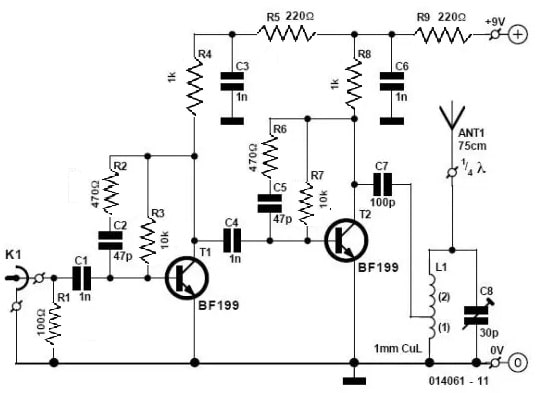
Booster Circuit for Cable Radio
Working Principle
The circuit operates using a 9 V battery or a suitable regulated DC power supply. Its approximate current consumption is 2.5 mA, depending on the component values and operating conditions.
The input signal is connected to the circuit through the coaxial connector. The two BF199 transistors amplify the received RF signal through successive amplification stages.
A tuned circuit consisting of an inductor and capacitor provides frequency selection and impedance matching. The C8 trimmer capacitor can be adjusted to obtain the required tuning response.
The output signal is coupled to the antenna through the output network. The antenna can then radiate the amplified RF signal, subject to applicable radio-frequency transmission regulations.
For better performance, it is recommended to construct the circuit on a properly designed printed circuit board (PCB). RF circuits are sensitive to unwanted capacitance, inductance, and electromagnetic interference.
During construction, follow these guidelines:
- Keep RF signal connections as short as possible.
- Use a large ground plane to improve circuit stability.
- Position the components according to the circuit layout.
- Keep the coaxial cable connection short.
- Avoid unnecessary wiring around the tuned circuit.
- Ensure that the inductor and capacitors are properly connected.
The L1 inductor can be constructed using approximately 1 mm enameled copper wire wound into three turns around an 8 mm diameter former.
Note: The circuit should be designed and operated in accordance with local RF transmission regulations. Do not assume that a particular transmission range or antenna arrangement is permitted.
Simple FM Transmitter Circuit using BF199
The BF199 transistor can also be used in a simple FM transmitter circuit. This circuit demonstrates how an NPN RF transistor can generate and amplify a radio-frequency signal.
Components Required
The main components required for this circuit include:
- BF199 NPN transistor.
- 3 V CR2025 battery.
- 100 kΩ resistor.
- 10 kΩ resistor.
- 56 pF capacitor.
- 47 pF capacitor.
- Inductor L1.
- Antenna.
- Audio input source.
- Connecting wires.
Connect the components according to the circuit diagram.
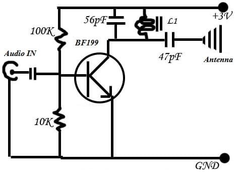
Simple FM Transmitter Circuit with BF199 Transistor
Working Principle
The circuit uses the BF199 transistor as an RF oscillator and modulation stage. A suitable LC network determines the oscillator frequency.
The inductor and capacitors form a tuned circuit that establishes the operating frequency. An audio input signal is applied to the transistor’s appropriate input connection, where it influences the RF signal to produce frequency modulation.
The generated RF signal is coupled to the antenna through the output connection.
The L1 coil can be constructed using approximately 36 SWG enamelled copper wire, wound into 2.5 turns around a suitable 5 mm diameter former, as specified by the original circuit design.
The circuit is compact and can operate from a low-voltage battery supply. However, its actual frequency stability, output power, and operating range depend on the circuit layout, component tolerances, antenna arrangement, and transistor characteristics.
Important Construction Precautions
- Use a suitable base-biasing resistor.
- Keep RF connections short.
- Avoid unnecessary parasitic capacitance.
- Use stable capacitors in the tuned circuit.
- Verify the oscillator frequency using suitable RF test equipment.
- Follow local regulations governing FM transmission and unlicensed radio devices.
The circuit is useful for understanding basic RF oscillation and frequency modulation principles. Any practical transmitter must comply with the applicable radio-frequency regulations.
Connecting a base resistor to the base terminal of the transistor is mandatory to avoid it being damaged. So, please refer to this link for: Choosing Base Resistance for Transistors in Electronic Circuits.
How to Test a BF199 Transistor Using a Multimeter?
Testing a BF199 transistor with a digital multimeter helps determine whether its semiconductor junctions are functioning correctly.
Since the BF199 is an NPN transistor, its base-emitter and base-collector junctions should behave similarly to two individual silicon diodes.
Follow these steps:
Step 1: Identify the transistor terminals
First, identify the collector, base, and emitter terminals using the manufacturer’s datasheet. Do not assume the pin arrangement based only on the package shape.
Step 2: Set the multimeter
Set the digital multimeter to diode-test mode.
Step 3: Test the base-emitter junction
Connect the red probe to the base terminal and the black probe to the emitter terminal.
A typical silicon junction should show a forward voltage drop, generally around 0.6–0.7 V, depending on the device and test current.
Reverse the probes. The multimeter should normally display an open-circuit indication.
Step 4: Test the base-collector junction
Connect the red probe to the base and the black probe to the collector.
A forward voltage drop should normally appear. Reverse the probes to check for an open-circuit indication.
Step 5: Check for collector-emitter shorts
Measure between the collector and emitter terminals in both probe directions.
A short-circuit reading in both directions may indicate a damaged transistor.
Note: These tests provide a basic indication of transistor junction condition. They do not verify the transistor’s current gain, leakage current, RF performance, or transition frequency. For more accurate testing, use a transistor tester or suitable semiconductor measurement equipment.
Advantages of the BF199 Transistor
The BF199 transistor provides several advantages in RF and high-frequency electronic applications.
- High-frequency operation: Its transition frequency makes it suitable for RF and IF amplification.
- Low collector capacitance: Its relatively low capacitance is beneficial in high-frequency circuit designs.
- Signal amplification: It can amplify weak electrical signals when correctly biased.
- Compact package: Its small package allows easy integration into compact electronic circuits.
- Low-power operation: It is suitable for circuits that require relatively low operating currents.
- Versatile applications: It can be used in radio receivers, RF amplifiers, oscillators, and other signal-processing circuits.Simple circuit integration: Its three-terminal configuration makes it convenient to use in conventional transistor circuits.
- No moving parts: Its semiconductor construction provides reliable operation without mechanical components.
Disadvantages of the BF199 Transistor
Despite its advantages, the BF199 transistor also has some limitations.
- Limited collector current: It is not suitable for driving high-current loads.
- Low power handling: Its maximum power dissipation restricts its use in high-power applications.
- Voltage limitations: Its maximum voltage ratings must be carefully observed.
- Thermal sensitivity: Excessive operating temperature can affect its performance and reliability.
- RF layout sensitivity: High-frequency circuits require careful PCB design and component placement.
- Manufacturer variations: Electrical characteristics may differ between manufacturers and device variants.
- Limited switching applications: It is not intended to replace power transistors in high-current switching circuits.
BF199 Transistor Applications
The BF199 transistor is used in several electronic applications that require high-frequency signal amplification and processing.
Its common applications include:
- RF signal amplifiers.
- Video intermediate-frequency amplifiers.
- Television receiver circuits.
- Radio-frequency receiver circuits.
- FM radio circuits.AM oscillator circuits.
- RF oscillators.
- Low-power FM transmitter experiments.
- Audio preamplifier stages.
- Signal amplification circuits.
- Wireless communication experiments.
- Electronic DIY projects.
- High-frequency signal-processing circuits.
- Radio and television IF amplifier stages.
Frequently Asked Questions About the BF199 Transistor
1. What type of transistor is the BF199?
The BF199 is an NPN silicon bipolar junction transistor primarily designed for radio-frequency and intermediate-frequency amplification applications.
2. What is the maximum collector current of the BF199 transistor?
The commonly referenced maximum collector current is 25 mA. However, the exact rating should be verified using the datasheet of the specific manufacturer.
3. What is the maximum collector-emitter voltage of the BF199?
The commonly referenced maximum collector-emitter voltage (VCEO) is 20 V. Always check the manufacturer’s datasheet before designing a circuit.
4. What is the transition frequency of the BF199 transistor?
A commonly listed transition frequency is 275 MHz. However, specifications can vary between manufacturers and device variants.
5. What are the equivalent transistors of the BF199?
Some potentially related or alternative transistor types include BF197, BF198, BF200, BF203, 2N9018, and C3355. Their electrical characteristics and pin configurations must be checked before substitution.
6. Can the BF199 transistor be used as an amplifier?
Yes. The BF199 can be used as an RF amplifier, IF amplifier, and signal amplification stage when properly biased and connected in a suitable circuit.
7. What is the package type of the BF199 transistor?
The BF199 is commonly available in a TO-92 through-hole package. However, the actual package should be confirmed from the manufacturer’s documentation.
8. What are the main applications of the BF199 transistor?
The BF199 is commonly used in RF amplifiers, video IF amplifiers, radio receivers, television circuits, oscillators, and other high-frequency electronic applications.
For additional information, refer to the BF199 Transistor Datasheet.
The BF199 is an NPN silicon bipolar junction transistor primarily designed for RF and IF signal amplification applications. Its high-frequency characteristics, relatively low collector capacitance, and compact package make it useful in radio receivers, television circuits, RF amplifiers, oscillators, and electronic projects.
Understanding the BF199 transistor pinout, electrical specifications, working principle, and operating limitations is essential when designing or troubleshooting electronic circuits. Its equivalent transistors can provide alternatives in certain applications, but their voltage ratings, current gain, transition frequency, power dissipation, and pin configurations must be verified before replacement.
By following the recommended operating conditions and consulting the appropriate manufacturer’s datasheet, the BF199 can be used effectively in a wide range of low-power, high-frequency electronic applications.