A bipolar junction transistor is a silicon-made electronic component where holes and electrons are used as charge carriers. This transistor allows a small current at one of its terminals to control a large amount of current supplying between the other terminals so that the device is capable of performing amplification or switching. BJT can be formed with three semiconductor material layers which are available in two types PNP and NPN. So the NPN transistor includes two N-type semiconductors and one P-type semiconductor where the P-type is sandwiched between two N-type semiconductors. Here, electrons are the majority charge carriers in NPN while holes are the majority charge carriers in PNP. This article discusses an overview of one of the types of NPN transistors namely 2N3563 Transistor, pinout, specifications, circuit, working, and its applications.
What is a 2N3563 Transistor?
The 2N3563 is a bipolar junction transistor, used as an oscillator, multiplier, and RF amplifier. Generally, it is an NPN type of transistor, available in TO-106 through-hole package, thus P-type semiconductor is sandwiched in between two N-type semiconductors. It is a semiconductor device, used to amplify or switch electrical signals as well as power. Its collector current ranges from 1.0 mAmps to 30 mAmps.
While looking for a suitable transistor for your application based on a few factors, it is very important to look into a few points on How to Select a Transistor.
Working
2n5415 transistor works on an amplification principle which means a small amount of current at the single terminal is utilized to control a huge current at the remaining two terminals. So, it is an NPN transistor, used mainly for low-power and general-purpose amplifying & switching-based applications. The three terminals of this transistor are used in the electronic circuits for external connection. These three terminals are dissimilar in terms of size and doping concentration.
Once the voltage is supplied at the base terminal, then it gets biased & starts drawing a small amount of current to control large current at the emitter & collector terminals. The voltage at the base terminal has a large effect on the output current attained at the collector terminal. So this procedure is used for amplification purposes.
Pin Configuration:
The pin configuration of the 2N3563 transistor is shown below. This transistor includes three terminals like a bipolar junction transistor which are explained below.
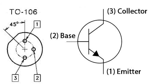
2N3563 Transistor Pin Configuration
- Pin-1 (Emitter): It emits all the charge carriers.
- Pin-2 (Base): This terminal is used to bias the transistor. It transmits all the charge carriers from the emitter terminal to the collector with minimum loss.
- Pin-3 (Collector): It gathers all the charge carriers from the emitter.
Features & Specifications:
The features and specifications of the 2N3563 transistor include the following.
- N3563 is a three-terminal NPN-type transistor.
- It is available in the TO-106 package.
- The transistor material is Si.
- Its collector to emitter voltage or Vce is 12Volts.
- Its collector to base voltage or Vcb is 30 Volts.
- Its emitter to base voltage or Veb is 4Volts.
- Collector current or Ic is 0.05 Amps.
- Collector power dissipation or Pc is 0.2 Watts.
- Its transition frequency is 600 MHz.
- Its collector capacitance or Cc is 1.7 pF.
- Maximum operating junction temperature or Tj is 125 °Centigrade.
- Its transition frequency or ft is 600 MHz.
- The minimum forward current transfer ratio or hFE is 30.
Equivalent & Complementary Transistors
The equivalent 2N3563transistor is BF158, S2C2570, MPS3563, SK3018 and TIS62 transistors. The complementary 2N3563 transistor is a 2N5415 PNP transistor.
Replacing a suitable transistor in any circuit based on requirement is very important. To know how to replace it, please refer to this; Replacing Transistors in Electronic Circuits: Factors and Considerations.
Crystal Oscillator Tester Circuit with 2N3563 Transistors
In modern electronics, tester’s requirements are increasing gradually. Similarly, a crystal oscillator tester is a type of tester used to test the crystal. Here we are going to design a crystal tester circuit with required components. The required components to make this crystal tester circuit include; a 9V battery, 1N4148 diode, 2N3563 transistor, capacitors, LED, resistors, and Crystal. Connect this simple circuit as per the diagram shown below.
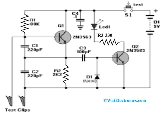
Crystal Oscillator Tester Circuit with 2N3563 Transistors
Working
Here the basic crystal oscillator tester circuit is designed with basic electronic components. So the connections of this circuit are very simple even an electronic beginner can also design this circuit & analyze it. This crystal oscillator tester circuit is very helpful as compared to conventional tester circuits due to its simple design & economic balances. This circuit works with a 9V battery which provides power supply to the crystal oscillator tester circuit.
1N4148 Diode
A 1N4148 is a standard silicon-based switching signal diode, used for upto 100 MHz switching applications. This diode in this circuit is used for very fast switching purposes and also protects circuit protection with high-speed rectification.
2N3563 Transistors
This circuit uses two 2N3563 transistors. This circuit is designed in such a way that whenever a crystal comes in contact with the whole circuit as well as the transistor, then this circuit will function & output whether the crystal we utilized here is good or bad. So transistors play a major role in this circuit without which the circuit is incomplete.
Capacitors & Resistors
The capacitor is a charge storage device, used widely in various applications. The main function of the capacitor in this circuit is to resonate with the crystal inductance to make the crystal oscillate. The resistors in this play a key role by limiting the current supply within the circuit.
Crystal
The crystal is the main testing component in this circuit that exhibits piezo-electric properties. So this property is exhibited whenever mechanical stress is provided across one of the crystal faces, and then a potential variation is developed across the opposed faces. Whenever a potential variation is provided across one of the faces, then mechanical stress is generated along with the other faces. So this effect is called as piezoelectric effect that can be observed in the crystal. The most frequently used crystal is the quartz crystal due to its strong nature, availability & low cost.
LED
LED or light emitting diode is a semiconductor diode that glows whenever a voltage is applied. So the LED in this circuit is connected simply in series with a transistor and a resistor. Here LED plays a major role because it indicates whether the crystal is in good or bad condition.
Once the circuit connections are made using the above components according to the above design, the circuit will be ready. When the good crystal is brought near to the circuit, then the LED in the circuit will glow to indicate that the crystal is in good condition. Similarly, when a damaged crystal is brought near to the circuit, then the LED in the circuit will not glow, so it indicates that the crystal is not good. Thus, this is the overall crystal oscillator tester circuit design and it’s working.
Connecting a base resistor to the base terminal of the transistor is mandatory to avoid it being damaged. So, Please refer to this link for; Choosing Base Resistance for Transistors in Electronic Circuits.
2N3563 Transistor Advantages & Disadvantages
The advantages of the 2N3563 transistor include the following.
- This transistor collector-emitter breakdown voltage is 12V.
- Its DC gain or hFE is 20 at 8mA & 10Volts.
- It can be utilized in all-purpose applications.
- These are smaller as compared to vacuum tubes.
- They utilize less power.
- They have a longer lifespan.
- These transistors are more rugged and can be used in ICs wherever a lot of transistors are fabricated above a single chip.
The disadvantages of the 2N3563 transistor include the following.
- This transistor is very sensitive to temperature.
- It cannot be operated above the 15 kHz switching frequency.
- These transistors can be broken because of the second breakdown or thermal runaway.
- Its reverse blocking capacity is extremely low.
- Its output voltage cannot be easily changed thus; the DC output voltage is not changeable.
- This transistor has less thermal stability.
- It is very effective through radiation.
- They generate noise.
- Its switching time is not extremely fast as compared to a higher alternating frequency of voltage and current.
2N3563 Transistor Applications
The applications of the 2N3563 transistor include the following.
- The 2N3563 can be used as an oscillator, multiplier, or RF amplifier.
- It can be used in a variety of electronic circuits for switching, amplification & signal-processing applications.
- This is a Si-type small signal NPN transistor mainly designed for general-purpose amplifier applications.
- This transistor is designed mainly for low-power electronic circuits.
- It can be used commonly as an NPN RF amplifier.
- This can be used in a variety of applications like; audio amplifiers, switching circuits, oscillator circuits, and small-signal amplification stages.
Please refer to this link for the 2N3563 Transistor Datasheet.
Thus, this is an overview of the 2N3563 transistor, pinout, features, specifications, circuit, working, advantages, disadvantages, and its applications. Thus, the 2N3563 transistor provides reliable performance for switching and amplification purposes within electronic circuits. Here is a question for you, what is 2N5415 PNP transistor?