MOSFETs are among the most widely used semiconductor devices in modern electronic circuits because of their high switching speed, low power consumption, and efficient current handling capability. Among different MOSFET types, N-channel MOSFETs are highly preferred in switching and logic-level applications due to their lower ON resistance and faster electron mobility compared to P-channel devices.
The BS170 MOSFET is a popular small-signal N-channel enhancement-mode MOSFET designed for low-voltage and low-current switching applications. It is commonly used in microcontroller interfacing, logic-level shifting, relay driving, LED control, motor switching, and signal amplification circuits. This MOSFET provides reliable switching performance with low gate drive requirements, making it suitable for hobby, educational, and industrial electronic designs.
This article discusses the BS170 MOSFET in detail, including its pin configuration, working principle, features, specifications, equivalent components, advantages, disadvantages, level-shifting circuit, and practical applications.
What is BS170 MOSFET?
The BS170 is an N-channel MOSFET that is produced by using DMOS technology and high cell density. This MOSFET is designed with the high-density procedure to reduce on-state resistance and provides reliable, rugged & very fast switching performance. So this MOSFET is used in most applications that require up to 500mA DC and also for low current and low voltage applications which include; power MOSFET gate drivers, switching, and small servo motor control applications.
BS170 MOSFET is manufactured using DMOS technology that provides low ON resistance, fast switching speed, and reliable performance for low-power applications. This higher technology has been adapted to reduce conduction loss, resist extreme dv/dt rate, provide advanced switching performance, and superior avalanche energy.
Pin Configuration:
The pin configuration of BS170 MOSFET is shown below. This MOSFET includes four terminals Drain, Gate, Source, and body or substrate. But this MOSFET works as a three-terminal device because the body area is attached always to the source terminal.
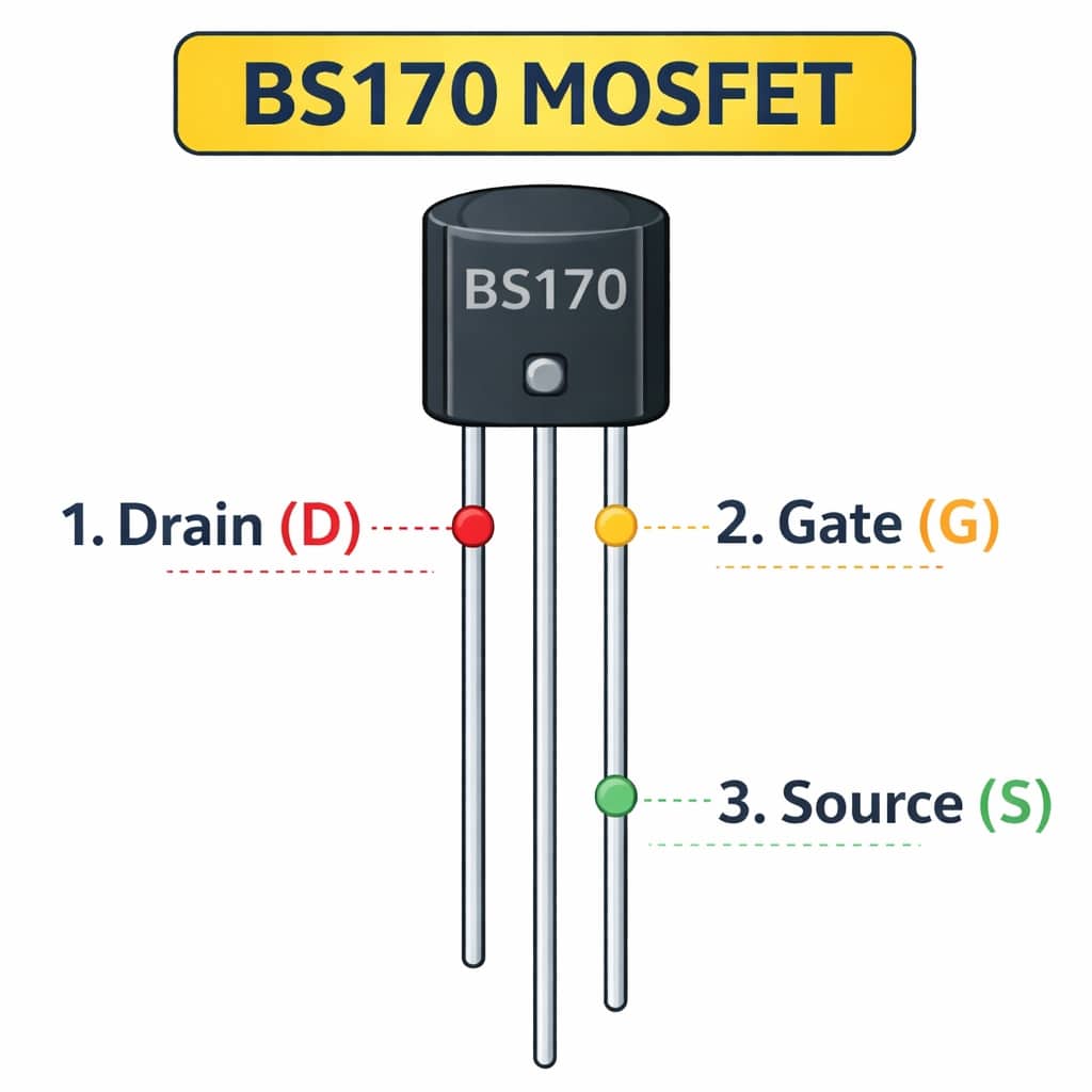
- Pin-1 (Drain (D)): It is a Drain terminal where the current flows throughout this terminal.
- Pin-2 (Gate (G)): It is a gate terminal that is used to turn ON the MOSFET. This terminal controls the current supply between the drain and the source whenever we apply the voltage supply on the gate terminal.
- Pin-3 (Source (S)): It is a source terminal where the current flows out throughout this terminal.
Features & Specifications
The features and specifications of BS170 MOSFET include the following.
- BS170 MOSFET is a Pb-Free device.
- It has low offset & error voltage
- This MOSFET is driven easily without any buffer.
- It has high high-density cell design to reduce ON-state resistance.
- It is used as a small signal voltage-controlled switch
- It is particularly for low current and low voltage applications.
- It has a high saturation current ability
- These are reliable and rugged.
- Its switching speed is fast (TON = 4ns)
- Its drain to source voltage or VDS is 60 V.
- Gate to source voltage or VGS; Continuous is ±20 V and Non-repetitive is ±40 Vpk.
- Its drain current or ID; continuous is 500mA and non-repetitive is 1200mA.
- Its low On-resistance is 2.5Ω.
- This MOSFET low input capacitance is 22pF.
- Its maximum lead temperature mainly for soldering is 300℃.
- Its turn time or TON and turn time or TOFF is 4 to 10ns.
- This MOSFET operating & storage temperature ranges from -55 to 150℃entigrade.
Equivalent & Alternatives
Equivalent BS170 MOSFETs are; 2N7000, VQ1000J, 2N7002, IRLML2502 and VQ1000P.
Alternative BS170 MOSFETs are; ND2406L, BSN20BK, VN1310N3P015, VN1710LP018, MPF6659, SST4118T1, BS208, SD1106DD, BSS7728E6327, 2SK1585, etc.
How to Securely Long Run BS170 MOSFET in a Circuit?
To get stable and long-term performance within a circuit by using BS170 MOSFET, it is recommended to not drive any load > 60V & 500mA. So the Gate terminal to Source voltage must be below ±20V. Do not operate & store this transistor in temperatures <-55 Celsius & > +155 Celsius.
5Volts to 3.3Volts Level Converter with BS170 MOSFET
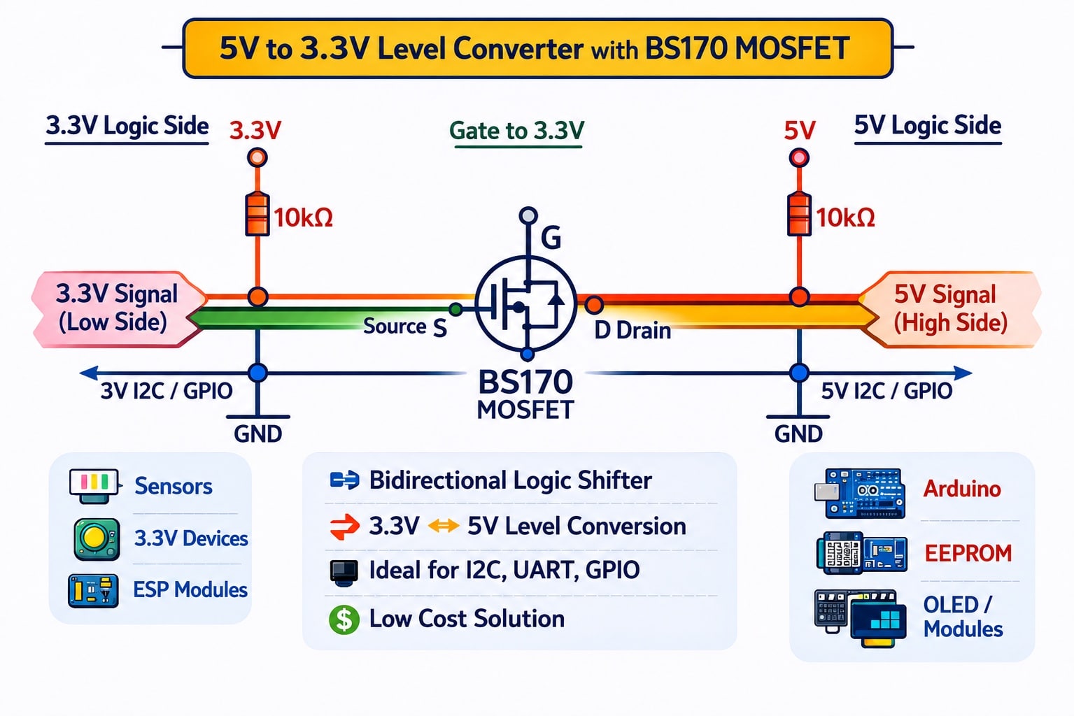
The 5Volts to 3.3Volts level converter with BS170 MOSFET circuit is shown below. The required components to build this circuit mainly include; two 4.7k resistors and BS170 N channel MOSFET.
This circuit is constructed with two 4.7k pull-up resistors. The source and Drain pins of MOSFET are pulled up toward the preferred voltage level for the low-level to a high-level (or) high-level to low-level logic conversion. Here for R1 and R2 resistors, you can use any value that ranges between 1k to 10k. In the below circuit, 5V & 3.3V of constant voltage are provided to the R1 and R2 resistors. The Low_side_Logic_Input & High_Side_Logic_Input pins can be used interchangeably as Input & Output pins.
Working
This circuit works in two conditions that need to be met when designing the circuit. So the primary condition is 3.3V low logic voltage level needs to be connected through the MOSFET’s source terminal. The 5V high logic voltage level should be connected to the drain terminal of the MOSFET. So the secondary condition will be, that the gate terminal of this MOSFET requires to be connected to the 3.3V low voltage supply.
In high to low-level logic conversion, the Logic input pin will be shifted between 5V & 0V and the logic o/p can be obtained as 3.3V & 0V. In this condition, if the MOSFET low side changes from a high to a low state, then it starts conducting. So the source terminal is in logic 0, thus the high side will become 0. Likewise, in the low to high-level change, the logic input ranges between 3.3V & 0V which is changed into 5V & 0V logic output.
Conditions
Once the above two conditions are fulfilled, then this circuit works within three conditions like the following.
Whenever the low side of MOSFET is in logic 1 (or) 3.3V.
When the MOSFETs low side is in logic 0 (or) 0V.
Once the MOSFET’s High side alters the condition from 1 to 0 (or) high to low from 5V to 0V.
When the MOSFET’s low side is high then it does not conduct because the Vgs threshold point of transistor is not attained. The gate terminal of the MOSFET at this point will be 3.3V & the source terminal is also 3.3V so, Vgs will be 0V and MOSFET will be off. High state or Logic 1 of the low side input reproduced on the drain terminal of the MOSFET as a 5V o/p through the R2 pull-up resistor. In this condition, if the MOSFET’s low side changes its condition from higher to low, then it starts conducting. So the source is in logic 0, and the high side will become 0.
So the above two conditions will convert voltage from a low logic state to a high logic state.
One more working condition is whenever the MOSFET high side changes its condition from high to low then the drain substrate diode will start conducting. So, MOSFET’s low side will be pulled down toward a low voltage level until the Vgs cross the threshold point is achieved.
Advantages & Disadvantages
The advantages of BS170 MOSFET include the following.
- The BS170 MOSFET is durable, reliable, inexpensive, robust, and an excellent choice,
- It performs fast switching and switches load within around seven nanoseconds because of which it can be utilized in high-speed circuits.
- This MOSFET’s very high-density process minimizes on-state resistance.
- Its advanced technology reduces conduction loss and provides better switching performance.
- It gives a robust thermal performance.
The disadvantages of BS170 MOSFET include the following.
- This MOSFET needs an isolated power supply or a bootstrap circuit to switch ON, this increases the difficulty of gate driver design. So this can lead to more space usage and design effort.
- This MOSFET is unstable when overload voltages occur.
- These are vulnerable to break by electrostatic charges because of the thin oxide layer.
- Its lifetime is short
- This MOSFET needs good designed circuit to perform well.
- Its operation speed is slow due to very high capacitive loading.
- This MOSFET has a large propagation delay on each gate
- It has high power dissipation as compared to CMOS.
Applications
The applications of BS170 MOSFET include the following.
- BS170 MOSFET is used within fast switching and drives loads below 500mAmps.
- It is used in audio amplification and Pre amplification purposes.
- This MOSFET is used within the o/p of microcontrollers and ICs.
- It is utilized in different kinds of signal amplification.
- It is used within electronic equipment and industrial automation for machine controls, vision controls, and light barriers.
- This MOSFET is utilized in battery-operated systems, solid-state relays, and drivers like solenoids, relays, lamps, displays, hammers, transistors, memories, etc.
- It is used in direct logic-level Interfaces like; CMOS or TTL.
Please refer to this link for the BS170 MOSFET Datasheet.
The BS170 MOSFET is a compact and efficient N-channel enhancement-mode transistor widely used in low-power electronic switching applications. Due to its fast switching speed, low gate drive requirement, and simple interfacing capability, it becomes an excellent choice for microcontroller projects, logic-level conversion circuits, signal amplification, and small load control systems.
One of the major advantages of the BS170 MOSFET is its ability to operate efficiently in both analog and digital circuits while maintaining low power loss and reliable switching performance. Its compatibility with logic-level signals makes it highly useful in Arduino, ESP32, Raspberry Pi, and other embedded system applications.
Although the BS170 is not suitable for high-current power applications, it remains a dependable and cost-effective solution for low-current control and switching designs. With proper gate protection, thermal management, and voltage limitations, this MOSFET can provide stable long-term operation in a wide range of electronic projects.