In the digital chip design, microcontroller applications and operational amplifiers, the open collector outputs are commonly used either for driving high loads such as relays or for interfacing with other circuits. As we know that BJT is a transistor and it has three terminals (Emitter, Base and Collector) where these terminals can be configured mainly in three switching modes. Those are Common Base, Common Collector and Common Emitter modes. Today, we are going to discuss about open collector configuration, its TTL gate, characteristics and advantages.
What is an Open Collector?
Open Collector is the general output where one can find in various integrated circuits. The open collector configuration operates like a switch which is either ground connected or disconnected. Other than connecting the output of an IC or any other transistor to specific device, it is connected to the NPN transistor’s base terminal where the collector is open and emitter terminal of the NPN transistor has internal connection with the ground pin.
So, the Open-collector’s output is considered as NPN transistor which allows current sink to common. For this open-collector circuit, there has to be a source for proper functioning of the output. When we require to calculate the output voltage when not hooked to any supply, then there will be no variation in voltage. The voltage at the output has to be calculated to know proper functioning of the open-collector circuit.
The circuit can offer either current sinking or current sourcing output based on the type of transistor (NPN or PNP).
- When the NPN transistor works on ‘’HIGH” condition, it offers sinking current to ground and in “LOW” condition, the output terminal will float until it is connected to the positive supply voltage using a pull-up resistor.
- When the PNP transistor works on ‘’HIGH” condition, it offers sourcing current to ground and in “LOW” condition, the output terminal will float until it is connected to ground using a pull-down resistor.
The below picture is the open collector circuit using an NPN transistor.
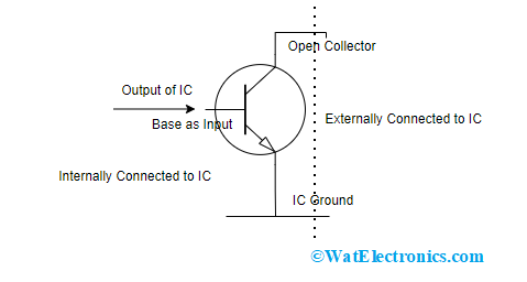
Open Collector IC
Open Collector Transistor Operation
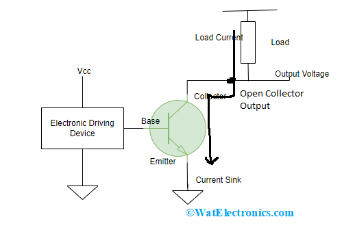
This section explains how does an open-collector work along with the circuit explanation. The switching circuit is mainly helpful for switching applications and for driving electromechanical kind of appliances. The PNP/NPN transistor’s base terminal can be either connected to analog or digital circuit and the emitter terminal has connection with ground. Whereas the collector terminal has connection with the switching load.
In the case of NPN transistor, when the base terminal is supplied with a control signal, the transistor moves to ON state. As the output is at collector terminal, the output gets pulled to ground through the conducting transistor junctions by energizing the load and making it ON. So, the transistor modifies and passes the load current which can be known through Ohm’s law where
Load current = voltage value at load section/resistance across load section.
Whereas when the NPN transistor’s base drive is in OFF condition, then the load will not get conducted and gets turned OFF. Then the transistor’s output helps in regulation of external load where the current-sink switching functionality of the transistor operates either as short circuit or open circuit.
Transistor Circuit Of Open Collector
The benefit in the open-collector transistor configuration is no necessity of connecting the collector load voltage to be at the same level of voltage potential of transistor’s driving circuit where it can be either high or low.
Open Drain vs Open Collector
The below tabular column specifies the differences between open drain and open collector configurations.
| Open Drain | Open Collector |
| The output is a form of FET transistor circuit. | The output is a form of bipolar junction transistor circuit. |
| It is termed as unconnected drain terminal of a P/N type FET transistor. Due to this external circuits can be connected so that it switches to ground in active state. | It is termed as unconnected collector terminal of a PNP/NPN transistor. Due to this external circuits can be connected so that it switches to ground in active state. |
| The output of the transistor drives supply voltage to output devices only if pull-up resistors are connected to the drain terminal. | The output of the transistor drives supply voltage to output devices only if pull-up resistors are connected to the collector terminal. |
TTL Gate of Open Collector
When transistor Tc is removed from totem-pole configuration, then an open collector TTL gate is formed. A TTL NAND gate can be transformed into AND gate by using a pull-up resistor in between the output terminals P and Q in the below picture.
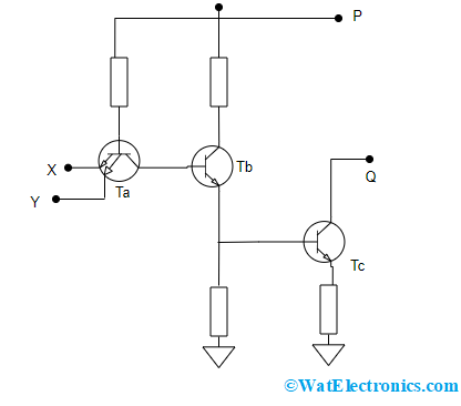
Open Collector NAND Gate
Using an open collector logic gate, wired AND and wired OR gates can be developed. In the below figure, multiple AND gates are ANDed with the help of open-collector TTL gate which shows the result as wired AND. This is because AND is produced by ANDing all the outputs which can be expressed as follows:
X = (U.V)’ (W.X)’ (Y.Z)’
When all the NAND gates collector terminals are shorted for the output transistors, this performs ANDing operation. Through this wired OR connection can also be obtained through DeMorgan’s principle and the equation is
X = (UV + WX + YZ)’
In the below figure the pull-up resistor value is known by the maximum value of current that flows across the collector terminal allowed via every output transistor.
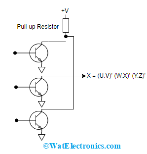
Wired AND-OR Using TTL NAND Gate
Examples
Open collector circuits are commonly used in voltage comparators. Few of the voltage comparator chips are of LM339, LM393 and LM311 where all these operate as open collector devices.
When any device which is connected at output , the output device should be connected to the positive voltage source that should be able to drive the load.
For example: When the output device is 12 V DC motor, then the output should have connection to +12V. Then, the load’s negative and ground terminals are connected to output of the device which drives the motor.
When a 12V DC motor has to be connected to LM311 chip, then the configuration is shown as follows:
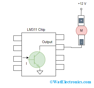
LM311 Chip With Open Collector Output
Advantages and Disadvantages
Here, the open collector advantages and disadvantages are discussed.
Advantages
- The foremost benefit of open collector circuit is that the load which has to be either controlled/switched can have connection with independent voltage supply. Or it can be varied from the supply voltage employed by the controlling circuit.
- These devices can be used for interfacing various families of devices which have various functional voltage levels.
- This device have the ability to operate with high voltage levels than that of chip supply voltage.
- Used for connecting multiple devices to single interrupt request signal or to a common bus in I2C circuits. This shows the result of enabling of only one device having no involvement of various inactive devices.
Please refer to this link to know more about Open Collector MCQs
Drawback
The drawback of open collector is high power consumption. This is because pull up resistor in the circuit uses power when the output is pulled to LOW state. This shows for required functional speed, and when the resistor value is low then the pull-up becomes stronger resulting in high power consumption.
This is all about the concept of open collector. The article has provided information on open collector configuration, working, TTL gate, advantages and drawbacks. Know open collector characteristics and how does those show impact on functionality of the device?