We all know that logic gates are the devices that stand as functional blocks for many of the digital circuits. Nearly 90%of the electronic devices are designed with logic gates to perform logical operations in those devices. These logic gates are dependent on Boolean algebra where those will generate output depending on the combination of digital signals from the input bits. Based on the kind of logic and the inputs combinations, the result will vary. The one type of logic gate which we are going to discuss today is OR gate. So, this article provides detailed inputs on its functionality, its truth table, OR gate benefits, and drawbacks.
Define OR Gate?
The output for a OR logic gate can be defined as LOW when all the inputs are at logic LOW. It can also be stated that the OR gate provides HIGH output when any of its inputs is at logic HIGH. The boolean expression for this gate is termed as Logical Addition which is represented with + sign and the logical expression is
Z = X+Y
So, OR gate can be exactly termed as Inclusive OR gate because it gives TRUE output when both the inputs are TRUE.
Theory
To have a clear understanding of the OR functionality, let us know how an OR gate performs corresponding to its inputs.
Consider there are two binary inputs, ‘0’ and ‘1’. As the OR gate operation is based on binary addition. So, when ‘0’ is added with ‘1’, or ‘1’ is added with ‘0’ the output is ‘1’ or when ‘1’ is added with ‘1’ The output is ‘0’ only when ‘0’ is added with ‘0’. That is
0 + 0 = 0
0 + 1 = 1
1 + 0 = 1
1 + 1 = 1
The symbol of the OR type logic gate is shown below:
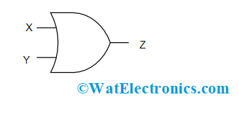
Basic OR Gate
Here, X and Y are considered as inputs and Z is the output. The X and Y inputs can be either ‘0’ or ‘1’.
It may have multiple inputs but has only one output. With this, the logical formula is given as
X + Y = Z
All the combinations of X and Y are represented in a tabular format which is the OR gate truth table, and it is shown below. The truth table shows the result of corresponding digital logic for all the possible input combinations. Here,
| X | Y | Z |
| 0 | 0 | 0 |
| 0 | 1 | 1 |
| 1 | 0 | 1 |
| 1 | 1 | 1 |
The above truth table is for a 2-input OR kind of logic gate. For example, the below picture shows the OR gate operation when it has three inputs then the logical representation and truth table are represented as follows:
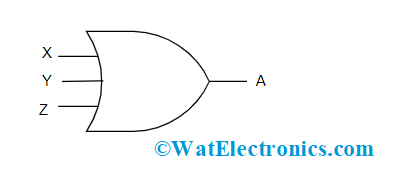
3 Input OR Gate
X + Y + Z = A
The logical diagram is
The truth table when OR logic gate has three inputs, and one output is:
| X | Y | Z | A |
| 0 | 0 | 0 | 0 |
| 0 | 0 | 1 | 1 |
| 0 | 1 | 0 | 1 |
| 0 | 1 | 1 | 1 |
| 1 | 0 | 0 | 1 |
| 1 | 0 | 1 | 1 |
| 1 | 1 | 0 | 1 |
| 1 | 1 | 1 | 1 |
Multi-input OR gate
The below picture shows how an OR logic gate is constructed with multiple input bits.
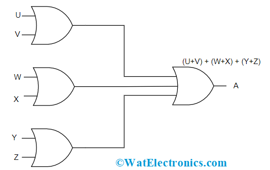
Multi Input OR Gate
Consider we have 6 inputs as U, V, W, X, Y and Z. Then the output is
A = (U + V) + (W + X) + (Y + Z)
When an OR logic gate with odd inputs is required, then a few of the inputs are made unused. The unused pins are connected to the ground directly using pull-down resistors.
Logic Gate OR Functionality
The below sections describe the functionality of OR gate using universal gates, diodes, and transistors.
Operation of OR Gate using Diode
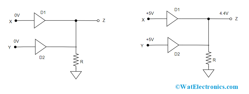
Below is the circuit diagram that shows OR logic gate operation using diodes.
OR Gate Using Diodes
As per the above circuit diagram, when the inputs X and Y are provided with 0V, then the output X shows no voltage. Whereas when either of the inputs is provided with a supply voltage of +5V, then the corresponding diode moves into forward biased condition and operates as a short, circuited device. So, the +5V voltage appears at output Z which means the output is logic HIGH.
In practical scenarios, the entire supply voltage +5V will not be present at the output, some level of voltage drop (0.6V – 0.7V) happens at the diode and the rest of the voltage level (4.3V or 4.4V) passes to an output pin. This 4.4V or 4.3V is ideally taken into consideration as logic HIGH.
When both the inputs are provided with a supply voltage of +5V, both the diodes will move into forward-biased state. Then the 4.4V voltage appears at the output. When both the inputs are grounded or provided with 0V, then there will be no voltage at the output and considered as logic LOW.
OR Gate using Transistor
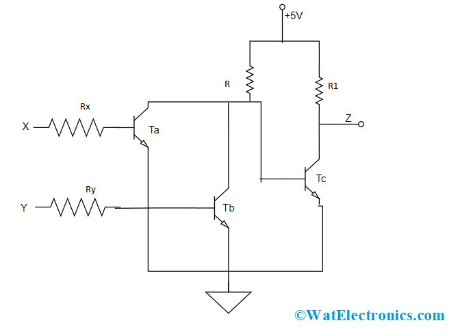
The operation and construction of an OR logic gate can also be derived using a transistor. Below is the circuit diagram of a two-input OR logic gate using a transistor.
OR Gate Using Transistors
Case 1:
When the input pins X and Y are provided with ‘0’ Volts or when both the pins are grounded, then the transistors TA and TB move into OFF condition correspondingly. At this condition, the supply voltage of +5V will not have a path to pass to the ground via any one of the transistors TA and TB. This makes the transistor TC get the required amount of potential and it will be in an ON state. Here, +5V voltage moves to the ground through R1 and transistor TC. As the third transistor TC is in ON condition, it performs as short-circuited device and the entire +5V gets dropped down to the ground and output appears to be logic LOW (0V).
Ideally, the transistor TC has some voltage drop (0.6V – 0.7V) across it and this voltage appears at the output which is considered as 0.
Case 2:
When both the input pins X and Y or either of the inputs is applied with high logic (+5V) which means the base terminals of both the transistors have +5V voltage. This makes the transistors TA and TB or either of the transistor to be in an ON state. Here, the supply voltage will find a path to the ground terminal through both the transistors TA and TB or either of them.
Then, current starts to flow to the ground via this path and the +5V will be dropped down at resistor R. This makes that transistor TC does not receive enough potential and it will be in OFF condition. So that the supply voltage will appear at the output which is logic HIGH or logic 1
This is the working scenario of the OR type of logic gate using transistors.
OR gate using NAND Gate
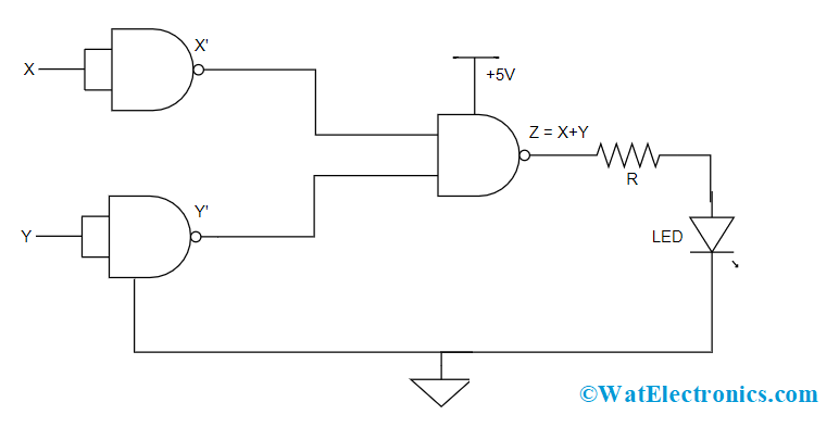
To implement an OR logic gate using the NAND gate, it is suggested to know about DeMorgan’s theorem. This theorem states that the product of the complement of inputs is equal to the complement of the sum of the inputs. This can be represented as:
OR Using NAND
(XY)’ = X’ + Y’
As per the above circuit, two NAND gates are used where the input terminals of both gates are shorted. This gives the output as X’. Y’
Then this output is provided as input to other NAND gates where this provides the result as (X’ + Y’)’
- [(X’). (B)]’
- (X’)’+ (Y’)’
So, the result is the sum of two inputs which is
X + Y
OR using NOR Gate
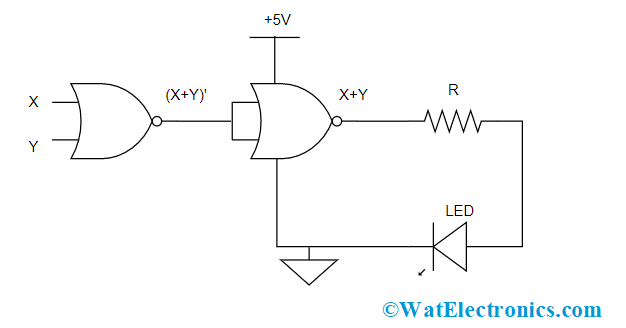
The below picture shows the arrangement of the OR gate using NOR gate.
OR using NOR
OR Gate ICs
OR gate ICs like IC 4071 and IC 7432 are discussed below.
IC 4071 – CMOS OR with 2-input
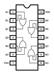
IC 4071 has 14 pins where four number of OR logic gates are used having two inputs for each gate. The 14th pin is a Vcc terminal where the maximum supply voltage is given to this pin so that the IC gets activated and the 7th pin is connected to the ground.
- Pins 1 and 2 are inputs for gate 1 and pin 3 is the output for the 1st gate.
- Pins 5 and 6 are the inputs for gate 2 and pin 4 is the output for the 2nd gate.
- Pins 8 and 9 are the inputs for gate 3 and pin 10 is the output for the 3d gate.
- Pins 12 and 13 are the inputs for gate 4 and pin 11 is the output for the 4th gate
With this arrangement, this IC appears internally as CMOS.
IC 7432 – TTL 2-input OR
In TTL logic, the IC of the OR type gate is 7432. This is a 2-input gate low-power Schottky version of OR. In addition to this, the other type of TTL logic OR logic gate is 74HC32 where VC represents high-speed CMOS. The 7432 IC has 14 pins, and the below picture shows the pin diagram.
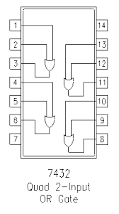
IC 7432
- Pins 1 and 2 are inputs for gate 1 and pin 3 is the output for gate 1.
- Pins 4 and 5 are the inputs for gate 2 and pin 6 is the output for gate 2.
- Pins 9 and 10 are the inputs for gate 3 and pin 8 is the output for gate 3.
- Pins 12 and 13 are the inputs for gate 4 and pin 11 is the output for gate 4
The 14th pin is a Vcc terminal where the maximum supply voltage is given to this pin so that the IC gets activated and the 7th pin is connected to the ground. When the supply voltage is more than the +SVDC voltage, then it may cause damage to IC.
Integrated Circuits
OR gate is present in both CMOS and TTL logics where TTL stands for Transistor-Transistor logic and CMOS stands for complementary MOSFET ICs. This section describes on what are the various configurations of OR gates with the TTL and CMOS logic.
IN CMOS logic, the OR gates are available from the 4000 series. This means
- 4071 is CMOS OR gate with 2-inputs.
- 4075 is the CMOS OR gate with 3-inputs.
- 4072 is the CMOS type OR gate with 4-inputs.
IN TTL logic, OR gate series is available in 7000.
- 7432 is the TTL type of OR gate which is a quad two-input OR gate that is this IC has four OR gates.
VHDL Code for OR Gate
library IEEE ;
use IEEE.std_logic_1164.all;
entity OR is;
port (X : in_logic; // input for OR gate
Y : in_logic; // input for OR gate
Z : out_logic); // output of OR gate
end OR;
architecture Logic of OR is
begin
Z <= X OR Y;
end OR;
Advantages and Disadvantages
Here, are the OR gate advantages and disadvantages.
Advantages
- The benefit of using OR type of logic gate is that it finds the maximum number in between the two inputs that are binary in nature.
- These are available in both TTL and CMOS logic
- Using NAND and NOR configurations, OR gates can be easily derived
- This gate functionality is also observed in ICs of P or N-type only transistor processes
- Here, multiple signals can be connected to output which has no impact on the other results
Disadvantages
- It has limited functional voltage values
- Sometimes there might time delay between input and output
Applications of OR Gate
The main applications of OR logic gate are:
- These are used in circuits where various power sources are available to perform the similar action
- Implemented in alarm systems and intrusion detection equipment’s
- Used in industrial plants for some protective measures
This is all about the concept of OR logic gate. This article has provided a detailed explanation of how an OR gate performs, its circuit diagram, truth table, gate ICs, examples, and applications. Also, know what is wired-OR gate using open-collector NOR gates?
