The transistor is a three-terminal semiconductor device, used as an amplifier or a switch. Generally, it is of PNP or NPN polarity but available in different types with different switching speeds and power ratings. If a transistor is designed to handle >1Amp of collector current, then it is considered normally to be a power transistor. So such transistors should have low output resistance to carry large load currents and good junction insulation to oppose high voltages. So, they should also dissolve heat very quickly to keep them from overheating. This article discusses an overview of the BD679 Transistor which is designed for use in switching and medium power linear applications.
What is the BD679 Transistor?
BD679 is an NPN-type silicon epitaxial-base Darlington transistor available within the TO-126 or Jedec SOT-32 package. This transistor includes two bipolar junction transistors connected within a single package which results in extremely high output gain. The maximum gain (Hfe) of this transistor is 1000 which makes this NPN transistor perfect for higher gain applications.
Its maximum collector current is 4Amps and the maximum peak collector current is around 6Amps. So, the maximum load voltage or CE voltage of this transistor is around 80V & the maximum collector dissipation of this transistor is around 40Watts. This transistor is used for a broad variety of general switching & amplification applications.
While looking for a suitable transistor for your application based on a few factors, it is very important to look into a few points on How to Select a Transistor.
How BD679 Transistor Works?
BD679 Darlington transistor includes two transistors effectively within the single package and also has very high gain & high current handling capacity, used in many applications. In the following circuit, the emitter terminal of the NPN transistor is connected to the negative rail which is known as the CE stage.
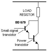
BD679 Transistor Working
In the above circuit, the higher transistor is a small-signal transistor where its collector and base terminals come out of the package. The lower transistor in the circuit CE leads coming out of the package. So the collector terminal is very common to two transistors.
Whenever a voltage supply is provided to the base terminal of this Darlington transistor then current supplies into the base terminal & turns ON the higher transistor. Now this pulling-up effect is transferred toward the base terminal of the transistor which is equivalent to increasing the base terminal with a hundred times more force than you used on the external base.
The transistor within the device very strongly pulls down on the base of the load resistor which allows a maximum voltage to emerge across the connected LOAD so the load will be activated.
Pin Configuration:
The pin configuration of the BD679 transistor is shown below. This transistor includes three terminals; emitter, base, and collector which are discussed below.
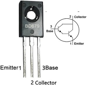
Pin Configuration
- Pin-1 (Emitter): This pin supplies the majority of charge carriers & also current drains out throughout this terminal.
- Pin2 (Collector): This terminal gathers the charge carriers from the emitter and a load is connected simply to this pin.
- Pin3 (Base): The base terminal is used to bias the transistor.
Features & Specifications:
The features and specifications of the BD679 transistor include the following.
- It is available in the TO-126 package.
- It is from the NPN family.
- It has three terminals like a BJT.
- Its maximum collector current IC is 4Amps.
- The peak collector current maximum is 6Amps.
- Collector to emitter voltage or VCE maximum is 80V.
- Collector to base voltage or VCB is 80V.
- The emitter to base voltage or VEBO maximum is 5V.
- Collector dissipation or Pc maximum is 40 Watts.
- The minimum and max DC gain or hFE is 1000
- Its maximum storage and operating temperature ranges from -65 to +150 Centigrade.
BD679 Transistor Internal Circuit
The internal circuit of the BD679 transistor is shown below. So, the BD679 transistor case has two transistors which are arranged on a single Si substrate with a protection diode and two resistors. All these components are simply connected to make an internal transistor circuit. So it is significant to recognize their existence so that you can utilize the transistor properly and know the component’s effect will have whenever the transistor is connected in any application.
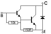
BD679 Transistor Internal Circuit
For instance, the 10k base resistor will react with the required current by the base terminal to turn on the transistor. Generally, 1uAmp current on the base terminal of a Darlington transistor would turn on the transistor. But here, a 10k base resistor reduces the resistance or input impedance of the base significantly so that a 1mA current is necessary. Most of the transmitted current into the base terminal is lost within the biasing network. Usually, this transistor is utilized within a high current part of a circuit, so these small losses are not important.
How to Long Run a BD679 Transistor in a Circuit very Safely?
To get a long-term performance of this component in a circuit, it is recommended not to utilize a component to its utmost ratings. Always utilize this transistor below 20% of its maximum ratings. So, the maximum collector current is around 4Amps thus do not drive any load above 3.2Amps. The maximum CE voltage of this transistor is 80V thus do not drive load above 64Volts. An appropriate heat sink must be used with this transistor and also always operate or store this transistor above -55 degrees centigrade & below +150 degrees centigrade temperature.
Equivalent & Complementary Transistors
Equivalent BD679 transistors are; 2SD1210, 2N6039, 2SD1514, 2SC2825, 2SD1515, 2SD1457, etc. The complementary BD679 NPN transistor is the BD680 PNP transistor.
Replacing a suitable transistor in any circuit based on requirement is very important. To know how to replace it, please refer to this; Replacing Transistors in Electronic Circuits: Factors and Considerations.
Bench Power Supply Circuit
The bench power supply circuit is shown below which is mainly designed for use in electronic experiment labs. This circuit is designed on a piece of copper laminate. This bench power supply circuit was designed mainly to use aged lantern “D” & “C” batteries. This circuit can produce at least 12v to 14volts from these batteries as well as cells. This simple circuit utilizes a board as a heat sink and enameled wire is utilized to connect different components. It can be bolted to keep the transistor very cool.
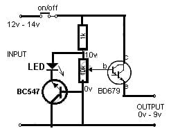
Bench Power Supply Circuit with BD679 Transistor
The Zener diode in the circuit is used to adjust the o/p of this power supply. Thus, there is a voltage of approximately 1.7 volts across a red color LED and also 8.2 volts between the BE terminals of a BC547. This circuit provides 0v to 9v at 500mA based on the life left within the used cells. Here, LED is used to specify the circuit is turned ON. The 10k potentiometer is utilized to regulate the output voltage.
Connecting a base resistor to the base terminal of the transistor is mandatory to avoid it being damaged. So, Please refer to this link for; Choosing Base Resistance for Transistors in Electronic Circuits.
6Volts – 12Volts Boost Converter Circuit
6Volts to 12Volts boost converter circuit design is shown below. This circuit is very useful if you have a 6V battery, although you need to utilize it for a 12Volts load such as LEDs. This circuit can also be known as a step-up converter but always the output current is lower as compared to input current.
The required components to make this circuit mainly include; 0.25W Resistors like; 1.8K, 4.7K, 1K, 1.5K, 33K, and 10K. Capacitors like 0.1µF 50V, 470µF 25V, diodes like; 1N4148, 1N5819 and 12V 0.5W zener diode, BC549/BC547, BD139/BD679 and 100µH to 220µH inductor. Connect this circuit as per the diagram shown below.
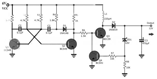
6Volts – 12Volts Boost Converter Circuit
Working
In the above circuit, the primary portion has transistors, resistors, capacitors, and a diode. All these components will be combined to make an astable multivibrator that gives a square waveform as an output which is a positive pulse signal at higher frequencies. After that, this signal is supplied throughout the R6 resistor to restrict a bias current throughout the Q3 base terminal. It makes the Q3 transistor function, thus higher current supplies throughout L1, and now the Q3 transistor performs as an on/off switch.
This characteristic can cause energy to build up within the L1 inductor & this energy can be produced throughout the D1 diode to rectify the current supply. In the C1 capacitor, the positive power is only chosen and stored which is an output. Thus it causes the output voltage to increase gradually. But whenever the output voltage enhances beyond VZ of ZD1 like 12V, then current is supplied throughout it and resistor R7 into the Q4 base terminal. So, this makes transistor Q4 to conduct.
Thus, the current supplying throughout R6 is pulled to supply throughout the pins collector and emitter of the Q4 transistor to the ground to turn OFF Q3. The voltage range at the output is decreased to 6V approximately because it is the flowing current throughout D1 & L1.
Whenever the voltage range is lower then there is no flow of current through the ZD1 diode so the Q4 transistor stops working. Again, current supplies throughout the R6 resistor and the base terminal of Q3. So this circuit continuously functions in these loops by maintaining the output voltage stable at 12V constantly. The C3 capacitor in the circuit works as a smooth filter to store electrical energy mainly for the load.
Advantages & Disadvantages
The advantages of the BD679 transistor include the following.
- BD679 transistor is a very handy component.
- This transistor has high gain & high current handling ability.
- It has two transistors within one package.
- The max gain of this transistor will make it perfect for higher gain applications.
- It has high protection and durability.
The disadvantages of the BD679 transistor include the following.
- When this transistor is within saturation region then there is no voltage drop across BE terminals.
- Its switching speed is not high.
- It has limited bandwidth.
- This configuration within a negative feedback circuit introduces phase shift at certain frequencies.
- It provides high power dissipation because of high saturation voltage.
- The leakage current of the first transistor is amplified by the second transistor. So its overall leakage current is higher.
BD679 Transistor Applications
The applications of the BD679 transistor include the following.
- BD679 transistor is used for any general-purpose switching & amplification purposes.
- Its maximum collector current is 4Amps which is capable of driving various loads like; motors, relays, transistors, etc.
- In addition, it can also be utilized at the o/p of electronic platforms like; Raspberry Pi, Arduino, etc.
- It can also be utilized to raise the gain of many types of signals such as audio and other electronic signals.
- It is used in motor driver circuits, BMS circuits, audio amplifier circuits, audio preamplifiers, switching or driving loads below 4A, and battery charger circuits.
- This series of transistors can be utilized as output devices within general−purpose complementary amplifier applications.
Please refer to this link for the BD679 Transistor Datasheet.
Thus, this is an overview of the BD679 transistor, pinout, specifications, circuit, working, and its applications. It is a three-layer NPN transistor where the collector current is a main function of the base current, so a change within the base current provides an equivalent amplified change within the collector current for a specified CE voltage. Here is a question for you, BD680 transistor?