Generally, the first letter of the transistor denotes the material, whereas the second letter denotes the type of device. SK and SL names within the transistor model refer to the package types. SL stands for a small outline, which indicates the transistor has a tiny and flat package with gull-wing-shaped leads. So SL100 is a common tiny outline transistor package. SK stands for small outline K, which indicates that this transistor has a tiny and flat package with flat and straight leads instead of gull-wing-shaped leads. So, SK100 is a common little outline K transistor package. Therefore, the first letter in the SK00 transistor indicates a Si transistor, whereas the second letter ‘k’ indicates a Hall Effect device. This article offers brief information on the SK100 transistor, pinout, specifications, circuit, working, and its applications.
What is an SK100 Transistor?
The SK100 is a three-terminal, PNP-type, and general-purpose medium power-based transistor, available in a TO-39 case. These transistor features mainly include: Simple drive requirements, High ruggedness, High secure operating area, etc. This transistor is used for amplification, switching, and regulation purposes. This transistor’s DC gain ranges from a minimum of 100 to a maximum of 300.
This transistor’s collector current is a main function of the transistor’s base current. So, this transistor works as a change within the base current and gives an equivalent amplified change within the collector current.
While looking for a suitable transistor for your application based on a few factors, it is very important to look into a few points on how to select a Transistor.
SK100 Transistor Pin Configuration:
The SK100 transistor includes three terminals: an emitter, a base, and a collector, which are discussed below. The emitter terminal is specified with a projecting edge within the transistor casing and is closest to the base terminal, and the collector terminal is at the reverse end of the casing.

SK100 Transistor Pin Configuration
- Pin-1 (Base): This terminal is used to bias the transistor, so when the base terminal gets enough voltage, a large current is supplied from the emitter to the collector terminal.
- Pin-2 (Collector): This terminal collects charge carriers and pushes through the emitter.
- Pin-3 (Emitter): This terminal attracts charge carriers from the collector throughout the base terminal and emits them.
Features & Specifications:
The features and specifications of the SK100 transistor include the following.
- SK100 is a three-terminal PNP transistor.
- It is available in a TO-39 metal case.
- It has a highly secure operating area.
- DC Current Gain (hFE): 40-300.
- Its collector−emitter voltage or VCEO is 50V.
- Its collector-to-base voltage or VCBO is 60V.
- Continuous collector current or Ic is 0.5A.
- Its emitter base voltage or VEBO is 5V.
- Its power dissipation or Pd is 800mW.
- Output capacitance is 20pF.
- DC gain or hFE ranges from 40 to 300.
- Operating temperature ranges from -65 to 200°C.
Equivalent & Complementary Transistors
Equivalent SK100 transistors are; 2SC9014, MJE13003D, 2N2907, TIP32, SL100, etc. A complementary SK100 transistor is the SL100 NPN transistor.
Replacing a suitable transistor in any circuit based on the requirement is very important. To know how to replace it, please refer to this; Replacing Transistors in Electronic Circuits: Factors and Considerations.
Burglar Alarm Circuit with Transistors
The burglar alarm circuit with two transistors is shown below. This circuit gives an alarm sound whenever the wire loop is broken. So the system is executed by simply installing a sensing loop that is mainly a thin copper wire. The loop is both invisible & brittle enough this way to break & initiate the alarm device easily.
The required components to make this burglar alarm circuit mainly include: transistors BC548and SK100, resistors like; 270 Kilo-ohm and 10 Kilo-ohm, 0.1μF, Ceramic disk capacitor, SPDT Toggle Switch, battery holder, 1Watt LS-4 (or) 8Ohm loudspeaker, battery holder and PCB. Connect this circuit as per the diagram shown below.
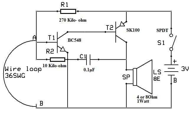
Burglar Alarm Circuit with Transistors
This circuit includes an oscillator section which is simply a two-stage amplifier through feedback. So this amplifier can be implemented using two transistors like; BC548 and SK100 which are connected within a feedback arrangement to produce oscillations. This T1 transistor is mainly responsible for generating oscillations while the T2 transistor is connected to the T1 base which amplifies these oscillations to drive the loudspeaker to generate the alarm.
The two transistors connection can be done in such a way that the T1 base terminal is shorted normally to the GND and when the sensing loop is unbroken it stays in the cut-off mode. Because of the lack of the base current within the T1 transistor, there are no oscillations so, the loudspeaker does not produce the alarm sound which indicates that there is no intrusion taking place.
Working
When an intrusion occurs, the loop will break and cause the loudspeaker to produce a continuous & loud alarm sound. When the loop is ruined the alarm can be silenced only by either deactivating the power supply. Once the loop is broken through a burglar, then the T1 transistor base terminal will become open & generate oscillations at its collector terminal.
When the base of the T2 transistor is connected to the T1 collector terminal, then oscillations are simply amplified through it & fed back further to its emitter terminal through the C1 capacitor & R1, R2 resistors path. Finally, the loudspeaker gets this amplified signal from the T2 transistor’s collector terminal and changes it into a clear alarm sound. So this indicates the incidence of an intrusion. Here, both the transistors are silicon type so the drawn current by this circuit is extremely low even within the alert mode.
Connecting a base resistor to the base terminal of the transistor is mandatory to avoid it being damaged. Please refer to this link for; Choosing Base Resistance for Transistors in Electronic Circuits.
Sound Operated Relay with Transistors
The sound-operated relay circuit with transistors is shown below. This circuit can be designed with different electronic components like; resistors like 47 kΩ, 5.6 KΩ, 3.3 KΩ, 820 Ω, 15 KΩ, 220 Ω, 4.7 KΩ variable resistor VR1 is 250 Ω, capacitors like 10 µF, 12V and 33 µF, 12V, transistors like AC126 PNP, SK100 or BC158 NPN, AC128 (or) AD149 PNP transistors, OA85 D1 Germanium Diode, X1 audio transformer, 8Ω LS1 loudspeaker, 6V Lamp and Motor. Connect the circuit as per the diagram shown below.

Sound Operated Relay Circuit with Transistors
Working
This sound-operated relay circuit is very simple to understand. So this circuit is designed with a two-stage audio amplifier using transistors. The sound sensor of this circuit can be done with 8Ω loudspeakers. This loudspeaker’s output is provided to the transistor’s base terminal through an X1 audio transformer for amplification. This amplified output can be provided to the input of the Darlington pair of T3 & T4 transistors.
If the sound wave is there, the Darlington pair will remain conductive & the drop across the emitter and collector terminals of the T4 transistor becomes very low this the load is energized. If the sound wave vanishes, then the load is de-energized.
Advantages & Disadvantages
The advantages of the SK100 transistor include the following.
- These transistors have high ruggedness.
- These are simple to carry and handle.
- These are small and lightweight.
- This type of transistor has very simple drive requirements.
- It has high secure operating region.
The disadvantages of the SK100 transistor include the following.
- These transistors are generally slow.
- Lateral transistors use a lot of space on a chip.
- These transistors have a large collector series resistance, thus they cause high-current effects at less collector current densities.
- The positive supply line in this transistor is a common point for mainly input & output current that results in a positive GND current. So this can be not convenient for design and maintenance.
SK100 Transistor Applications
The applications of the SK100 transistor include the following.
- The SK100 transistor is a medium-power and general-purpose transistor used for switching, regulation, and amplification purposes.
- SK100 medium power transistor is used in applications where BC547 is found insufficient.
- It is used for less distortion complementary designs.
Please refer to this link for the SK100 Transistor Datasheet.
Thus, this is an overview of the SK100 Transistor, pinout, specifications, circuit, working, and its applications. It is a three-terminal PNP transistor where the collector current is a main function of the base current, so a change within the base current provides a corresponding amplified change within the collector current for a specified collector-emitter voltage. This transistor is biased if there is a signal at its base terminal, then it completely remains on. If there is no signal at the base signal, then it completely gets off. Here is a question for you: What is BC548transistor?