NOR gate is a basic logic gate and is the inverse of the OR gate which performs different logical operations. This is the combination of NOT OR gates. Hence, it performs NOT and OR logic gates operations between a minimum of two binary inputs or more to provide an output binary signal. Generally, NOR logic gates are used to design latches and flip-flops. This gate combines both an OR gate and a NOT gate functionalities thus, frequently known as a NOT-OR gate. Examples of NOR gate ICs are CD4001, NTE4001, TC4001, HCF4001, etc. This article elaborates on CD4001 IC, pin-out, features, specifications, and applications.
What is CD4001 IC?
CD4001 is a single-chip CMOS integrated circuit which neither includes two input quad NOR gates internally. This IC is based on a monolithic CMOS transistor with efficient source and sink capabilities. So this IC is operated very easily in various applications This IC is available in a 14-pin DIP package which works up to 125 degrees temperature. This IC provides anti-interference, low power consumption, and strong flexibility. So it has leakage current drive and symmetrical source abilities which are compliant through CD4000 series ICs.
How CD4001 IC Work?
A Quad 2-Input NOR Gate IC like CD4001 IC includes four NOR logic gates independently on a single chip where each gate has two input pins and a single output pin. So every gate output is high only whenever its two inputs are low. When the voltage supply is provided to the suitable pins of the IC like pin-14 and pin-7 then the corresponding output pin generates a low or high logic level based on the NOR gate function.
NOR Gate
A NOR logic gate is a combination of an OR & NOT gate that combines both gates functionalities this gate is often known as NOT-OR gate. The NOR Gate truth table is shown below.
The NOR logic gate provides a HIGH output when all the inputs are LOW. Thus, if any one of the inputs of the gate is HIGH, then the output will be LOW automatically because the outputs of the OR logic gate can be inverted through the NOT gate.
CD4001 IC Pin Configuration:
The pin configuration of the CD4001 IC is shown below. So this IC includes 8 pins which are explained below.
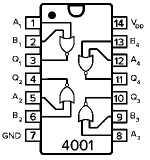
CD4001 IC Pin Configuration
- Pin-14 (VDD): It is a power supply voltage pin that supplies +3V to +15V.
- Pin-7 (GND): It is a power ground pin of IC.
- Pins 1, 5, 8 & 12 (A1 to A4): These are the Inputs-A of the NOR gates within the IC.
- Pins 2, 6, 9 & 13 (B1 to B4): These are the inputs B of the NOR gates within the IC.
- Pins 3, 4, 10 & 11 (Q1 to Q4 ): These are the output pins of the NOR gates in the IC.
Features & Specifications:
The features and specifications of CD4001 IC include the following.
- CD4001 is a standard CMOS IC.
- This IC is available in a 14-pin DIP package.
- This IC includes 14 pins.
- This IC includes neither 4-separate two-input NOR Gates.
- It has four channels.
- Its voltage supply ranges from 3V to 18V.
- This IC has two inputs for each channel.
- Maximum IOL is 6.8 mA.
- Maximum IOH is -6.8 mA.
- Its output type is Push-Pull.
- The input type is standard CMOS.
- The standard speed is tpd > 50ns.
- The maximum data rate is 8 Mbps.
- Maximum input leakage at 15V is 1 µA.
- The typical propagation delay time is 60 ns at VDD = 10 V and CL = 50 pF.
- Operating temperature ranges from -55 to 125°C.
Equivalents & Alternatives
Equivalent to CD4001 ICs are HCF4001, TC4001, MC14001, HEF4001, NTE4001, etc. Alternative to CD4001 ICs are 4572 IC & 74HC02 IC.
Electronic Letter Box Circuit with CD4001 IC
A simple electronic letter box circuit is shown below. This circuit is useful in indicating whenever mail is received through an LED. Generally, the LED in the circuit turns ON but whenever a letter is dropped into your letterbox by someone, the LED will stop glowing thus, it turns OFF. So that we can know that there is a letter within your letterbox.
The required components to make this circuit mainly include; a mini breadboard, 5V power supply, LM741 IC, CD4001 IC, resistors like 10KΩ and 1KΩ, capacitors 0.1μF and 1uF, an LDR, two LEDs and connecting wires. Connect this simple circuit as per the diagram shown below.
Principle:
The circuit working principle is very simple. Here an LDR and an LED are used in the circuit to recognize the presence of a letter within the box. LDR is a type of resistor where resistance changes based on the light-dropping intensity on it. In dark or low light conditions, its resistance will be around 2 Mega Ohm whereas, in bright light conditions, its resistance will reduce to a few Ohms. The LED in this circuit is used as a source of light.
Whenever the light falls on the LDR directly from the LED and whenever any letter is dropped in the letter box, then it will obstruct the falling light from the LED on the LDR. So this change can be noticed using supporting circuitry which includes CD4001 IC, 741 IC & an LED.
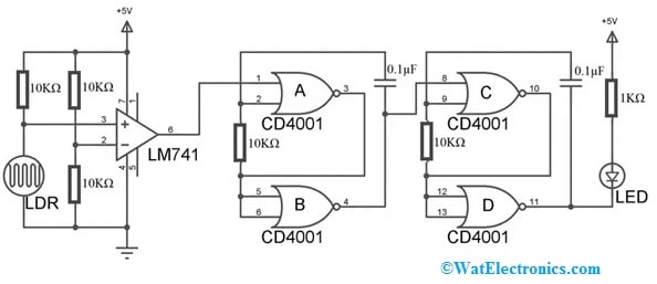
Electronic Letter Box Circuit with CD4001 IC
Working
This circuit working is very simple, so the LDR & the LED must be connected at the corners of the letter box so that the LED light will fall regularly on the LDR. Thus, the LM741 op-amp output signal will be HIGH.
This high output signal is provided to Pin-1 of CD4001 IC and it provides 1 as an output whenever all the inputs are low. So, the LED will glow continuously to know that there is no letter within the drop box.
If someone drops any letter within the letterbox, then the light dropping on the LDR will be blocked due to high resistance. So the Op-Amp output will become LOW which is provided to Pin-1 of CD4001 IC then we will get Logic 0 through output Pin-3. This, in turn, will obtain Logic 1 on the Pin-4 of the IC, because the inputs of the second NOR gate are provided from Pin-3. In the second gate both the inputs get logic 0 then the output will be HIGH at pin-4.
At last, the output at Pin-11 will be HIGH so, the LED will stop glowing so that we can know that there is a letter within the letter box. The LED will turn off until all the letters in the box are taken out. Once all the letters in the box are taken out then the LED will start glowing once more.
Advantages & Disadvantages
The advantages of CD4001 IC include the following.
- The CD4001 CMOS IC has a reliable, efficient design & adaptability.
- This integrated circuit includes four two-input NOR gates in a single package to simplify the development of digital logic circuits.
- It performs like a universal gate which amplifies its importance in crafting cost-effective and
- versatile solutions for both easy and difficult applications.
- This IC is a significant component that simply bridges innovation & functionality within modern electronics.
- This IC has low static power consumption.
- It operates with a voltage that ranges from 3V to 18V.
- This IC includes a diode that guards input terminals from fixed current interference.
- It is a flexible IC.
- It has a symmetrical source, leakage current drive, dynamic capability, etc.
The disadvantages of CD4001 IC include the following.
- CD4001 IC power rating is limited & cannot work at higher voltages.
- These are fragile, that cannot resist high-voltage operation.
- They generate more noise throughout the operation.
- These ICs are complex with a lot of components, making it hard to recognize & isolate defects.
Applications
The applications of CD4001 IC include the following.
- A CD4001 IC is used primarily in various logic circuit applications wherever a fundamental NOR gate function is required like simple logic operations, making more complex logic gates, building FFs, and many digital circuits, encoders, and decoders.
- These are frequently found in DIY electronic projects because of their low cost & versatility.
- It is a universal gate so any other logic gate can be designed with this gate within digital logic design.
- This IC has low power consumption, so used in battery-powered devices.
- It operates with a wide range of voltages, providing circuit design flexibility.
- This IC implements simple logic neither functions like AND NOT & OR NOT by merging several NOR gates.
- This IC designs multiplexer circuits to choose particular data inputs depending on control signals.
- It creates simple alarm logic wherever high output is produced only once several conditions are met.
- It controls the LED brightness with a combination of NOR gates to create a dimming effect. This IC is frequently used in beginner electronics projects because of its simplicity & availability.
Please refer to this link for the CD4001 IC Datasheet.
Thus, this is an overview of CD4001 IC from the CD4XXX IC series, pin-out, features, specifications, and applications. This is a 2-input Quad NOR Gate IC mainly designed to implement the complementary MOS technology. It is incorporated with P-type and N-type enhancement mode transistors. So this NOR gate IC allows designers to execute positive logic OR gate operation. Here is a question for you, what is TC4001IC?