After the development of the first point-contact transistor, the phototransistor was invented by one of the teams at Bell Labs. At that time, a large number of developments were being started. Even though the phototransistor history is not publicized like other early developments of semiconductors, but it was certainly a very significant development. The first invention of this transistor was announced on March 30th, 1950. This article discusses an overview of a phototransistor and its working.
What is a Phototransistor?
A semiconductor device like a phototransistor includes three layers with a light-sensitive base region. Here, the base region detects the light & changes it into the current that supplies among the two regions like the emitter & the collector.
The phototransistor construction can be done like an ordinary transistor apart from the base region. In this type of transistor, the flow of current to the base region is not provided, but the light energy can be used as the input.
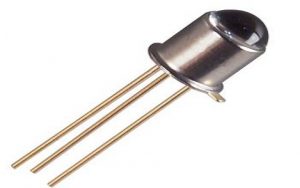
Phototransistor
Alternatively, a phototransistor is also considered like a Photodiode including a current amplifier. This transistor changes directly from photons to charge similar to a photodiode and also offers a current gain. The phototransistor symbol is shown below that is the same as an ordinary transistor but the main difference is that the two arrows on this will explain the light incident on the base terminal of the transistor.
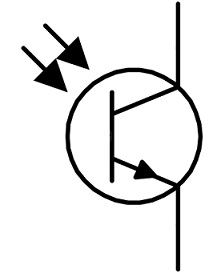
Phototransistor Symbol
Similar to normal transistors, these also include large gain except the size of the base to collector terminals. In this type of transistor, the base to collector junction size is higher because it is a light-sensitive area of the sensor.
When the size of the junction is higher, then it results in a significantly better junction capacitance. Consequently, these transistors have less frequency response as compared to photodiode despite the high gain.
Working Principle
The working principle of a phototransistor is similar to a photodiode including an amplifying transistor. The light falls on the base terminal of a phototransistor then it will induce a little current then the current amplified through the action of a normal transistor, which results in an extensively large. Generally, as compared with a related photodiode, a phototransistor generates 50 – 100 times of a photodiode current.
The phototransistor is fabricated with a semiconductor material. Once the light falls on the material then the charge carriers like holes or electrons of the semiconductor material can cause the current to supply within the base area. The base region of this can be used for transistor biasing.
The light penetrates the base terminal of the transistor to produce the pairs of electron-hole in the reverse biasing. The flow of electrons in the pressure of the electric field can cause the current within the base region. This current can be injected with the electrons within the emitter area. The main disadvantage of this transistor is the low-frequency response.
Phototransistor Construction
As compared to the normal transistor, the area of the collector and base terminals in the phototransistor is large. The best example of a phototransistor IC is the 2N5777 phototransistor.
The area of the base terminal can be increased to enhance the amount of produced current because when more light drops on this transistor then a huge current will be generated. Before, it was designed with a single semiconductor material such as germanium or silicon. At present, these transistors are made up of Arsenic & Gallium to get high efficiency.
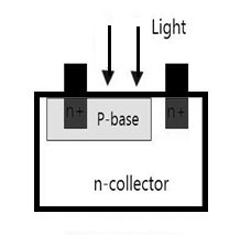
Construction of Phototransistor
At last, the arrangement of a phototransistor can be done in a metallic box & a lens is placed at the top of the box to absorb the incident radiation. The construction of the phototransistor is quite similar to the ordinary transistor. Earlier, germanium and silicon materials are used for constructing this phototransistor.
The junction of the emitter-base is connected in forwarding bias whereas the collector-base region is connected in the reverse biased. Whenever no light ray drops on the transistor’s surface, then a little reverse saturation current will induce on top of the phototransistor due to the fewer minority charge carriers.
The energy of light drops on the junction of the collector to base then it generates the majority charge carriers and adds the flow of current toward the reverse saturation current. The graph below shows the magnitude of current increases along with the intensity of light.
Characteristics
The characteristics of a phototransistor are discussed below.
In the following graph, the x-axis signifies the applied voltage at the collector-emitter region of the transistor whereas the y-axis signifies the collector current supplies throughout the device in mA. From the following graph, we can notice how the current flow in the collector region changes with the incident light intensity.
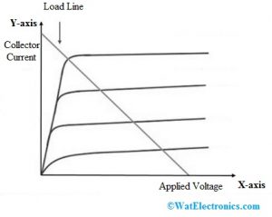
Characteristics
The current within the collector terminal enhances through the intensity of light. The current within the collector region changes through the wavelength as well as the light intensity. In the above graph, we can notice that the current increases through the light intensity when falls on the base terminal. And also signifies the difference within the base current through the difference within the intensity of light.
Difference between Photodiode and Phototransistor
The main difference between photodiode and phototransistor includes the following.
| Photo Diode | Photo Transistor |
| It is responsive more to incident light | It is not responsive more to incident light |
| The linear response is high, so used to measure the exact measurement of light | The linear response is low |
| It allows less current, so used in less power consumption applications | It allows more current, so used in high power consumption applications |
| It is not sensitive | It is more sensitive |
| Dark current is low | Dark current is high |
| It is not used as a solid-state switch | It is used as a solid-state switch |
| Operational speed is high | Operational speed is low |
| Noise interference is less immune | Noise interference is more immune |
| Output response is fast | Output response is low |
| The High-frequency response of this diode gives good results | The High-frequency response of this diode gives poor results |
| It is used to change the energy of light into current | It is used to change the light energy into current |
| It generates both current & voltage | It generates only current |
| It works in both biasing | It works in forward biasing |
| It is used in light meters, solar plants, etc | It is used to detect the light |
Simple Alarm Circuit
The circuit diagram of a simple alarm circuit using a phototransistor namely a light interruption alarm is shown below. By using this transistor, we can design this circuit. Once the light drops on this transistor, it will be activated & the gate region of the SCR will be LOW. So, the SCR will be deactivated.
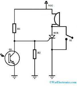
Simple Alarm Circuit
Once the light gets interrupted, the transistor will be turned OFF & provides sufficient potential on the gate terminal of SCR to activate it. Consequently, the alarm can be generated & it can be reset with the help of the switch.
Specifications
The specifications of the phototransistor include the following.
- Peak wavelength is 940 nm
- Max Power 100 mW
- The package is round with 5 mm
- Max Current is100 nA
- The type of lens is dark plastic to slash noticeable light
- Maximum Ic is 3.12 mA
- The viewing angle is 20 degrees
- Maximum VCE Breakdown is 30 V
Advantages
The advantages of phototransistors include the following.
- Highly sensitive
- Not expensive
- Less complex
- It provides a high amount of current including high gain.
- As compared with photodiodes, these transistors have high gain, current & quick response time.
- These are sensitive to wavelengths which range from UV to IR through visible radiation.
- Sensitive to different light sources like fluorescent, incandescent, lasers, sunlight, neon bulbs, flames, etc.
- Stable temporarily
- Reliable highly
- Less noisy as compared to avalanche-type photodiodes.
- These are available in different packages like transfer-molded, epoxy-coated & surface mounted.
Disadvantages
The disadvantages of phototransistors include the following.
- It gives a less frequent response.
- When the illumination is low then the circuit is not capable to notice it effectively.
- Electric surges occur frequently
- Phototransistors get affected by the difference within electromagnetic energy.
Applications
The applications of phototransistors are as follows:
- For light detecting and controlling
- In counting systems and punch card readers
- In relays
- Alarm Systems
- Level Indicators
- Proximity Detectors
- Encoders
Please refer to this for How to Select a Transistor.
Please refer to this link to know more about Phototransistor MCQs
Thus, this is all about an overview of a phototransistor and its working These are semiconductor devices & they are existing like PNP or NPN transistors. These components can also be available like other semiconductor devices & electronic components from almost all electronic component distributors with less cost. So, phototransistors are extremely sensitive and it is fairly slow. The major drawback of this transistor is increased sensitivity. Here is a question for you, what are the different types of transistors available in the market?