A boost converter is a DC-to-DC switching converter IC that efficiently increases the input voltage to a high output voltage. This voltage conversion is possible by storing energy in an inductor in the switch-on phase and releases to the load in the switch-off phase. So these are different kinds of DC-to-DC converters linear, switch mode, boost, buck, transformer-based buck-boost, and isolated. Power electronics applications need high output voltage as compared to the input source especially based on boost converters. Thus, this article elaborates on ME2108 IC, pin-out, features, and its applications.
What is ME2108 IC ?
ME2108 is a DC/DC step-up converter IC with low supply current through the CMOS process which produces a stable 5V DC output voltage. So the ME2108Xxx series ICs are suitable where low supply current & low noise are required like battery-powered devices, hand-held communication equipment, keyboards, wireless mice, cameras, toys, camcorders, PDAs, VCRs, etc. Thus, this converter IC is available with a chip enable (CE) function that reduces power dissipation in shut-down mode.
Thus, the ME2108 is a type of step-up DC-DC converter IC mainly designed to boost a voltage from a low input to a higher output efficiently. This IC has low power consumption and operates with low input voltages as compared to other ICs. So, the ME2108 IC is a dedicated boost converter including different features like low noise operation and programmable output voltage.
How ME2108 IC Works ?
The ME2108 DC/DC step-up converter IC works with a microchip like a switch to build up energy within a choke. Here the microchip works like a switch that works at 180 kHz high frequency. So, whenever the switch is closed, then the battery’s power will go to the choke wherever energy is stored. Once the switch is opened then surge voltage takes place, which is higher as compared to the voltage supply. So the energy stored within the choke can be rectified into a DC and stored within the parallel capacitors. Thus, the chip feedback keeps the voltage supply at 5 volts. Whenever a load is connected to the output of the converter then it is powered by the stored energy within the capacitors.
ME2108 IC Pin Configuration:
The pin configuration of ME2108 IC is shown below. This IC includes three pins which are discussed below.
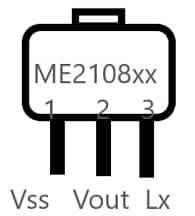
ME2108 IC Pin Configuration
- Pin-1(Vss): It is a ground pin of DC to DC switching converter IC.
- Pin-2 (Vout): It is an output pin of IC.
- Pin-3(Lx): It is a switch node pin of IC that works as a reference mainly for the floating top gate driver.
Features & Specifications:
The features and specifications of ME2108 IC include the following.
- ME2108 IC is a DC/DC PFM step-up converter IC.
- This IC includes three pins.
- It is available in SOT89-3 and SOT23 packages.
- Its operating voltage ranges from 0.9V to 6.5V.
- Output voltage ranges from 2.0V to 7.0V.
- Output voltage accuracy is ±2.5%.
- It has less ripple and noise with a low current supply through the CMOS process.
- The low start voltage is ≤ 0.9V at Iout=1mA.
- The typical maximum oscillator frequency is 180KHz.
- Output current Iout is 400mA if Vin is 3.0V & Vout is 5.0ZV.
- Its efficiency is high 85%.
Equivalents & Alternatives :
Equivalent to ME2108 IC includes; BL8530 IC, 6065 IC, ME2108A33PG & ME2108A50PG. So, alternatives to ME2108 ICs are; LM2596 IC, TC7660 IC, TC7660 IC, XL1509 IC, TC7662 IC, etc.
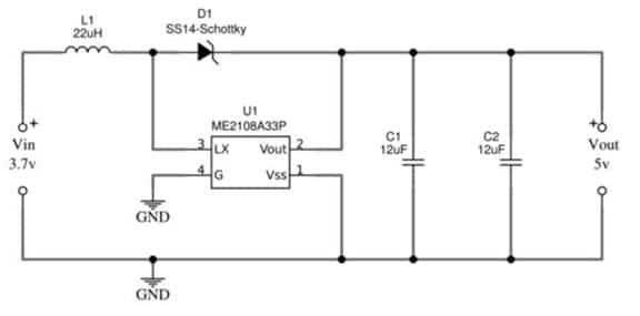
Boost Converter Circuit with ME2108 IC
Whenever we utilize a low-power controller or a microprocessor within the circuit, then we need to provide extra power sources to drive exterior components. Once we implement various power sources then the circuit design will become bulky & very complex by boosting the converter. So this is a DC-to-DC power converter used to increase voltage while decreasing current using its input supply toward its load. So here we are designing a 3.7V to 5V boost converter circuit using an ME2108 Series DC/DC step-up converter.
The required components to make this circuit mainly include; ME2108 IC, 22µH Inductor, SS14 Schottky diode, 12µF capacitor, 3.7V power supply, and connecting wires. So, connect this circuit as per the diagram given below.
IC ME2108 is a step-up DC/DC converter IC with a low supply current which decreases high frequency switching noise & output can be programmed in between 2.0Volts to 7.0Volts. Thus, this IC uses three external components only to turn into a step-up converter. So this IC can be utilized for battery-powered devices with a low current supply.
Boost Converter Circuit with ME2108 IC
Working
A boost converter circuit from 3.7V to 5V is mainly designed with an ME2108 DC/DC step-up converter IC with a low supply current. Generally, the DC power supply can be boosted with a high-frequency switching pulse. So this circuit utilizes a similar principle to bring higher output voltage using a low input voltage. This ME2108 IC decreases high-frequency switching noise where its output can be programmed in between 2.0V to 7.0V. So this ME2108 IC utilizes minimum external components because of the internal architecture.
This IC uses an Inductor at the input and a Schottky diode & Capacitors at the output. So this IC can deliver 400mA o/p current if the i/p voltage is 3.0Volts & the o/p voltage is fixed at 5.0Volts. This IC uses a maximum 180KHz switching frequency. Here the output voltage range can be changed by the Inductor & output capacitor values.
Thus, whenever you design the printed circuit board for the boost converter with ME2108 then need to set external components close enough and reduce the connection between the IC & components.
Advantages & Disadvantages
The advantages of ME2108 IC include the following.
- ME2108 IC decreases high-frequency switching noise.
- Its output can be programmed in between 2.0V to 7.0V range.
- It generates smooth waveforms.
- It has a high power density.
- This IC has high efficiency and less EMI emissions.
- It provides good isolation and gentle switching at higher frequencies
- It provides low noise and low ripple.
- Efficient power management
- It uses low-supply current & CMOS process technology to handle power efficiently.
- This IC can be utilized to design a high-efficiency and low ripple step-up DC/DC converter by using three external components only.
- The advanced circuit design of ME2108 IC reduces high-frequency noise throughout switching.
- The chip enables the function of this IC to decrease power dissipation in shutdown mode.
The disadvantages of ME2108 IC include the following.
- This IC has a high input current ripple.
- Capacitive turn-on losses can occur.
- Switching losses can occur at the turn-off
- These converters can cause noise throughout the operation.
- They can have high loess.
- These converters can have high input & output capacitance.
- The DC/DC converter’s circuitry can be costly.
- They provide an unsteady voltage & current supply.
Applications
The applications of ME2108 IC include the following.
- The ME2108 DC/DC step-up converter IC can be used to design a power bank.
- This IC can be used as a driver mainly for LED flashlights.
- It is used with battery-powered instruments that need low noise & low supply current.
- This IC can be utilized as a power source for different wireless devices like mice, keyboards, cameras, toys, etc.
- It is used as an LED driver, Hybrid electric circuit, LED backlight, solar power system, etc.
Please refer to this link for the ME2108 IC Datasheet.
Thus, this is an overview of ME2108 step-up power boost converter IC that provides stable 5V DC output voltage at different input voltages like 0.9Volts, 1.5Volts, 1.8Volts, 2.5Volts, 3Volts, 3.3Volts, 3.7Volts, 4.2Volts to 5Volts. This module’s starting voltage is 0.9V and the output current is 7mA which operates at 180 KHz frequency. Its typical conversion efficiency is approximately 85%. This IC can be used to design power banks and drivers for LED flashlights. This IC consumes different amounts of current to generate a balanced output for various input voltages. Here is a question for you, what is a buck converter?