The 4000 series CMOS logic family ICs were introduced first by RCA in 1968. These are lower-power alternatives to 7400 series TTL ICs with a binary counter & an oscillator. After that, it was migrated slowly into the 4000B buffered series in 1975. These ICs have a wider voltage supply range than the contemporary logic family. So, CD4060 IC is one of the 4000 series CMOS logic chips well-known for its high noise immunity and low power consumption. This article elaborates on the CD4060 IC, pin-out, specifications, working, and its applications.
What is CD4060 IC?
The CD4060 IC is a CMOS chip, available in different 16-pin packages like PDIP, SOIC, CDIP, TSSOP, etc. This IC’s operating voltage ranges from 3V to 15V. This IC includes a binary counter & an oscillator. So this IC produces selectable time delays and different frequency signals due to an in-built oscillator that needs only a few passive components.
In addition, we can also configure crystal oscillators through RC circuits or external crystals. This IC can also have a reset circuit, which makes the counter begin again from all zeros. The primary function of this IC is to generate customizable time delays to make it a practical choice in timing-related applications.
Pin Configuration:
The CD4060 IC pin configuration is shown below. So, this IC includes 16 pins, which are explained below.
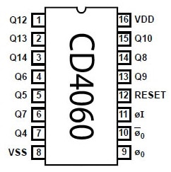
CD4060 IC Pin Configuration
- Pins 1 to 7 (Q3 to Q9): These are output counter pins of the IC.
- Pin–8 (GND): It is a power GND or 0V pin of the module.
- Pin-9 (CEXT): It is an Input connection pin used for an external capacitor.
- Pin-10 (REXT): This input connection pin is used mainly for external capacitor connection.
- Pin-11 (CLK11): It is a CLK input or oscillator pin of the IC.
- Pin-12 (RST12): This is a reset pin that resets the counter.
- Pins -13 to 15 (Q11 to Q13): These are output pins that counter outputs.
- Pins-16 (VDD): This is a power supply voltage pin that ranges from +3V to +15V.
Features & Specifications:
The features and specifications of CD4060 IC include the following.
- CD4060 is a 14-bit binary counter or divider IC.
- It is available in 16-pin CDIP, PDIP, TSSOP, and SOIC packages
- It’s counting in decimal ranges from 0 to 16383.
- Operating voltage ranges from 3V to 18V.
- Nominal voltage is 5Volts, 10Volts, and 15Volts.
- The maximum CLK frequency at 15V is 30MHz.
- The reset propagation delay at 5V is 25ns.
- Its operating temperature ranges from -55°C to +125°C.
How does CD4060 IC Work?
The CD4060 versatile CMOS IC works as a 12-bit binary counter with an in-built oscillator. So it generates a CLK signal & counts up within binary format with every falling clock pulse edge. Generally, this IC merges a binary counter & a built-in oscillator by allowing it to produce different frequencies or adjustable time delays through counting CLK pulses & incrementing its binary output with every falling edge.
The in-built oscillator module in the CD4060 IC is a binary counter, so the counter value will be incremented by 1 within binary numbers on every negative CLK pulse transition. Here, the reset input must always be connected to GND. If a HIGH (1) positive signal is provided to this input, then it resets the counter (or) oscillations to begin from starting. So reset value effect & CLK pulse are given in the following table where ‘X ‘in the table is the don’t care condition.
Tabular Form
The tabular form of CD4060 IC includes the following.
|
Transition |
RESET |
Counter Value |
|
X |
1 |
Reset Counter to zero value |
|
Negative Transition |
0 |
The counter value is advanced by one step. |
|
Positive Transition |
0 |
There is no change. |
The above Boolean logic table illustrates how the RESET value & CLK signal interact. So it displays how the counter performs in response to a variety of signals, which makes it easier to know & control the operation of IC
Equivalents & Alternatives
Equivalents to CD4060 ICs are; CD4017, CD4020, NTE4060, HCF4060, MC14060, TC4060, HEF4060, etc. So alternatives binary counters are; CD4024B (12-bit), CD4024B (7-bit), CD4020, CD4024, CD4040, etc.
Ni-Cd Reliable Battery Charging Circuit with CD4060 IC
Ni-Cd (Nickel-cadmium) batteries are normally found in gadgets and household electronics for stable charging & discharging. So here we are designing a Ni-Cd battery charging circuit to recharge your batteries safely with protection to keep everything running very smoothly.
This battery charger is mainly designed to charge seven Ni-Cd pencil cells within a series (or) a 9Volts Ni-Cd battery pack. So it works at a 50mA stable current with security indicators that notice short circuits, reverse polarity, and high resistance (or) low-voltage battery conditions, which are signaled throughout two LEDs.
After a 14-hour charging phase, the battery will be detached from the circuit and switched to drip charging mode to stop overcharging and keep the battery healthy. In addition, a clear alarm sound will be generated when the charging procedure is completed.
Components
The required components to make this circuit mainly include; Resistors like R1 – R4, R6, R7 (100 KΩ), R5-1 KΩ, R8 & R9 – 1.5 KΩ, R10 & R11 – 1 MΩ, R12 & R13 – 3.3 MΩ, R14 – 22 Ω/0.5W, R15-33 Ω/0.5W and VR1 – 100 KΩ. Capacitors like C1 – 0.01 µF, C2 & C4-0.22 µF, C5-220 µF, 25V and C6 – 0.1 µF. Semiconductors like IC1-CD4060 IC, IC2-LM317T, and IC3-µA741CN IC. T1 & T2 – BC547 NPN transistor, D1-1N4001 rectifier diode and D2-1N4148 signal diode. LED1 – Red and LED1 – yellow LEDs, PZ1-piezo buzzer and RL1-12V, 150Ω relay.
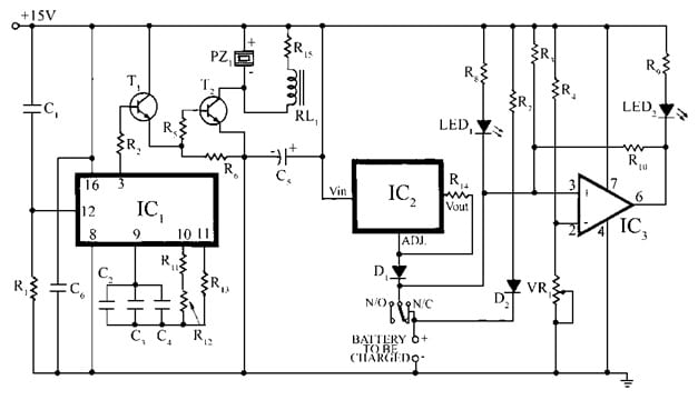
14-Hour Timer for Battery Charging Control Circuit
Working
The Ni-Cd charger circuit is separated into three main portions: a constant current source, a 14-hour timer, and a comparator circuit for monitoring the battery, which is explained below.
Constant Current Source for Battery Charging
This constant current source in the above circuit uses an LM317 IC, which provides a constant current. So by selecting the correct R14 resistor value, the output current will be set to 50mAmpos with I = 1.2V/R14 formula. To confirm the battery doesn’t discharge if there is a power breakdown, then D1 & D2 diodes are included for safety.
Here, the R7 resistor & D2 diode work mutually to permit trickle charging when the battery is completely charged. So a little current flows continuously by maintaining the battery refilled without any overcharging.
14-Hour Timer for Battery Charging Control
This circuit can be handled by CD4060 IC1 and a 14-stage counter is equipped through an oscillator. So this oscillator’s can be set through F = 1/2.2RC, wherever R => R11 + R12 & C => C2 + C3 + C4. So the oscillator runs with the values provided at 1/6 Hz, and pin-3 of this IC outputs a higher signal after 14 hrs, signaling the end of the major charging phase.
A Darlington driver in this circuit includes T1 & T2 transistors, which trigger the RL1 relay. It disconnects the battery from the main current source to avoid overcharging. Simultaneously, a buzzer rings to indicate that the battery is completely charged & ready to utilize. Here, the C1 capacitor & R1 resistor reset IC1 automatically throughout power-on.
Comparator for Monitoring Battery Health
The comparator in the above circuit uses µA741 IC to check the health of the battery by comparing different voltages through pin-2 by setting 0.4Volts through VR1. Here, Pin-3 is connected across the battery & generally stays connected to +Vcc throughout the R3 resistor. To maintain the circuit constant and keep away from any false readings, an R10 resistor is included to set up some hysteresis.
Conditions:
- If the RED color LED is ON and the yellow color LED is OFF, then it indicates normal Ni-Cd battery charging.
- If the RED color LED is ON, and the Yellow color LED is ON, then it indicates there may be a reverse battery connection. Make sure that the battery is properly connected. So, if the battery is properly connected, then the battery will be short and not work.
- If the RED color LED is ON, the Yellow color LED is ON for some time & goes OFF, then it indicates a low voltage battery; thus, charging will be continued.
- If the RED color LED is ON for a moment & after that goes OFF, then the Yellow color LED will be OFF. It indicates a high resistance battery, so the battery is not functional.
Conclusion:
This Ni-Cd battery charging circuit is versatile, which provides you with a consistent and efficient method to charge all types of Ni-Cd batteries. So this circuit is very simple to utilize with built-in security features like a trickle charging mode & an alert sound to allow you to identify whenever charging is finished. So it is a great choice for Ni-Cd batteries, however, you can also regulate it for other kinds similar to lead-acid. In addition, the stable current charging will confirm your batteries stay completely charged & last longer.
Advantages & Disadvantages
The advantages of the CD4060 IC include the following.
- The CD4060 IC is a versatile chip.
- This IC allows for precise & adjustable time delay generation.
- Its built-in oscillator allows the generation of a variety of frequencies with minimum external components.
- This IC needs a few passive components only for oscillator action, circuit design simplification & implementation.
- It has a 14-bit binary counter, which allows counting & dividing signals.
- This IC’s 12 output pins can be utilized to control a variety of functions.
- These are small in size, reliable, and consume less power.
The disadvantages of CD4060 IC include the following.
- The number of bits directly a counter IC handles will dictate its highest counting capacity.
- A binary counter is a digital circuit, so it is vulnerable to noise interference, which causes incorrect counting.
- These counters generate output within a binary format, so it might not always be the most appropriate for all applications.
- It has a limited counting range, the need for exterior circuitry for non-binary outputs, vulnerability to noise, and potentially increasing cost & complexity.
Applications
The applications of CD4060 IC include the following.
- The CD4060 IC generates precise & adjustable time delays, thus helping in building time-related circuits & timers in both consumer and industrial electronics.
- These are used in delay-inducing circuits in industrial automation, home security systems, etc.
- It is utilized to separate high-frequency signals into minor and more manageable segments, which is useful in a variety of frequency-related applications.
- This IC can also be employed to count operations or events that range from easy counting tasks to difficult industrial monitoring systems.
- This IC produces various outputs with different frequencies so used in audio & synthesizer projects.
- This IC is used to create time delays, counters, frequency dividers & other timing-related circuits.
- It is used in different timing & frequency generation applications.
- These are suitable for applications that need accurate & consistent timing.
Please refer to this link for the CD4060 IC Datasheet.
Thus, this is an overview of CD4060 IC, pin-out, features, specifications, circuit, working & its applications. This is a versatile IC that merges an oscillator & a counter, making it a great choice mainly for different tasks that require accurate & adjustable timing. Its simple design allows it to handle time delays efficiently, making it a popular choice for timing-related projects. So this IC is fairly simple to utilize and uses fewer passive components to make stable signals for different frequency & timing applications. Here is a question for you: What is CD4020 IC?