BC549 transistor is a semiconductor device and its main function is to switch or amplify electronic signals as well as electrical power. This transistor is composed of semiconductor material including three terminals that help in connecting to an external electronic circuit. Whenever voltage (or) current supply is provided to one terminal pair of the transistor then it controls the flow of current throughout the remaining terminal pair. Here, the output power is higher than the input power because it amplifies a signal. This article provides brief information on the BC549 transistor, pinout, specifications, and its applications.
What is a BC549 Transistor?
BC549 is a general purpose three terminal NPN transistor in SOT54 and TO-92 packages. This transistor is used for switching little loads, Darlington pairs, small-signal amplifiers, etc. BC549 transistor includes three layers one P-doped and two N- N-doped where the P-doped layer is arranged between the remaining two N-doped layers. In addition, this transistor has two PN junctions, so one junction is forward-biased and the second junction is reverse-biased. This transistor is a low voltage low power current controlled device, used mainly for amplification and switching purposes in various electronic circuits.
BC549 transistor is used in three configurations common emitter or CE, common base or CB, and common collector or CC, but CE configuration is used mostly for amplification purposes because it contains the precise voltage and current ratings necessary for amplification.
The amplification factor or beta (ß) is used mainly to describe the amplification nature. So, it is the main ratio between base and collector current. The amplification factor of this transistor mostly ranges from 420 to 800. The current gain or alpha (α) is another factor which is a ratio between emitter and collector current. This value ranges from 0.95 to 0.99.
BC549 transistor is accessible in various part numbers with current gain values. So BC549 current gain value ranges from 110 to 800, the BC549A transistor current gain is from 110 to 220, the BC549B current gain ranges from 200 to 450 and the BC549C transistor ranges from 420 to 800.
Working
Whenever a voltage supply is provided at the transistor’s base terminal then it gets biased & draws current to connect the emitter and collector terminals, so current starts flowing from the collector terminal to the emitter. Whenever no voltage is provided at the base terminal then it is known as grounded. So, the transistor in this case performs as an open switch wherever both the collector and emitter and stay open.
BC549 is an NPN transistor hence the collector and emitter will be left open (Reverse biased) when the base pin is held at ground and will be closed (Forward biased) when a signal is provided to the base pin. It is a low-current transistor hence the maximum amount of current that could flow through the Collector pin (Ic) is 100mA, hence we cannot connect loads that consume more than 100mA and load voltage more than 30V using this transistor. BC549 has a decent gain value hfe from 420 to 800; this value determines the amplification capacity of the transistor.
When this transistor is fully biased then it allows a maximum of 100mAmps to flow across the collector and emitter. This stage is called the Saturation Region. When the base current is removed the transistor becomes fully off, this stage is called the Cut-off Region.
While looking for a suitable transistor for your application based on a few factors, it is very important to look into a few points on How to Select a Transistor.
BC549 Transistor Pin Configuration:
BC549 transistor pin configuration is shown below. Understanding its pin configuration is very significant whenever it is connected to the circuit because it decides how this transistor works and changes signals (or) switches currents depending on the applied input to the transistor base terminal. This transistor includes three terminals which are discussed below.
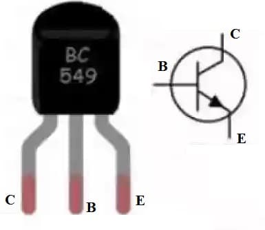
BC549 Transistor pin Configuration
- Pin- 1 (Collector): The collector terminal is a positive terminal that allows the current flow. It is connected to a connected load because it works like an output terminal.
- Pin-2 (Base): The base terminal is a control terminal that controls transistor biasing by turning ON/OFF this transistor. This pin performs as the input terminal.
- Pin-3 (Emitter): The Emitter terminal is a negative terminal that drains out current. It is connected normally to GND.
Features & Specifications:
The features and specifications of the BC549 transistor include the following.
- BC549 is an NPN transistor.
- It is available in the TO-92 package.
- The mount type is Through Hole.
- The maximum collector current or IC is 100mAmps.
- Collector to emitter voltage or VCE maximum is 30Volts.
- Maximum collector to base voltage or VCB is 30Volts.
- The maximum emitter to base voltage or VEBO is 5 volts.
- Collector dissipation maximum or Pc is 500 mW.
- The transition frequency or fT maximum is 150 MHz
- DC gain or hFE ranges from a minimum of 110 to a maximum of 800.
- Its storage and operating temperature must be a minimum of -65 to a maximum of +150 Centigrade.
- The saturation voltage from collector to emitter is 250 mV
- It has a single-element configuration.
- Its gain bandwidth is 300 MHz.
- The breakdown voltage maximum is 30 Volts.
Equivalent & Complementary Transistors
BC549 equivalent transistors are; BC548, 2N3904, 2N2222, BC550, PN100, C945 and BC337. The complementary BC549 transistor is the BC559 PNP transistor.
Replacing a suitable transistor in any circuit based on requirement is very important. To know how to replace it, please refer to this; Replacing Transistors in Electronic Circuits: Factors and Considerations.
How to safely use BC549 Transistor in a Circuit?
BC549 transistor is used long run securely in a circuit to get the best performance. So it is suggested not to drive any load above 100mA because if we drive a load > 100mA, it may harm the transistor or its performance may get weak. Do not drive any load >30Volts and need to use an appropriate base resistor always to protect the circuit from over current. Do not connect the transistor pins wrongly in the circuit and always it must be stored at a temperature >-65 centigrade and < +150 centigrade.
Intercom Circuit with BD140 and BC549 Transistors
An intercom is a two-way communication electronic device used to send and receive audio transmissions. This is also known as an intercommunication device, door phone, or talkback. This device is used in large homes when you want to speak with anyone from any other place in your home when you are very busy doing house tasks. This is a very convenient device to interact easily with each other within the home to avoid shouting or a walk.
A simple intercom circuit is shown below. This circuit can be built with different components like; 0.001uF and 0.1uF ceramic capacitors, 100uF electrolytic capacitor, BD140 & BC5493 transistors, resistors – 0.25W, 0.5W, 1 ohms, 1K, 150 ohms & 2.2M, switch, 0.25 watts 8 ohms Speaker, 4.5V Battery and a PCB. Connect this circuit as per the diagram shown below.
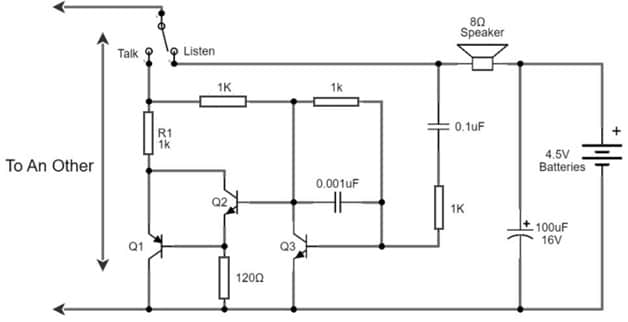
Intercom Circuit with Transistors
Working
The working of the intercom circuit is, that whenever the S1 switch is pressed to talk, it enables the circuit to function as the transmitter. Once you start speaking something into a loudspeaker then the inside coils of this speaker can cause an oscillation to produce a small signal. This signal will go into the capacitor C2 and R5 resistors. After that, this signal will go into the Q3 base transistor. Here both the Q3 & Q2 NPN transistors work a high-gain amplifier circuit.
This signal will be transmitted to drive the Q1 PNP transistor to control the flow of current to another one from the Intercom. At last, it will supply throughout the speaker in the receiver intercom circuit and it will also produce the sound signal. The 4.5-volt battery connected to this circuit does not influence anything through the speaker (or) the circuit due to DC voltage, so this voltage will be blocked through the C2 capacitor. The receiver circuit battery is a transmitter circuit power supply & a speaker is connected to only wires.
Here the work will exchange in between two circuits arranged at various elements of the house. Whenever one circuit works as a transmitter then another one works as a receiver. This circuit’s frequency operation mainly depends on the human spoken sound that ranges from 200 Hz to 3 kHz. This simple circuit can be arranged in small & quiet sufficient buildings.
Connecting a base resistor to the base terminal of the transistor is mandatory to avoid it being damaged. Please refer to this link for; Choosing Base Resistance for Transistors in Electronic Circuits.
High Impedance Preamplifier Circuit with a Transistor
A high-impedance preamplifier circuit with a transistor is shown below. Generally, impedance is an electrical component one of the characteristics that measure resistance to a current. But, impedance can be low or high medium.
Impedance plays a key role in impacting the ability of an output device. For audio amplifiers like headphones, high impedance is outstanding. Lower impedance-based devices may give less sound to listen to normally but resist playing deeper bass or higher treble. The amplitude may turn distorted at both limits of the frequency range. So, headphones with high impedance are distortion-free and generate very clear audio projection.
The required components to make this high impedance preamplifier circuit mainly include; BC549 NPN transistor, 1M, 4.7K and 100 ohm resistor, 10uF & 100uF electrolytic capacitor, and 0.1uF capacitor. Connect the circuit as per the diagram shown below.
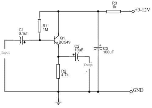
High Impedance Preamplifier with BC549 Transistor
Working
The high-impedance preamplifier circuit simply follows the emitter follower design wherever input is given throughout the transistor base terminal. The input is provided at the base terminal of the transistor whereas the output of this can be taken at the emitter pin. The power supply is provided to the collector pin throughout the R3 resistor and C3 capacitor.
Here, bias current is provided to the base terminal of Q1 throughout the R1 resistor and we connect the load across the R2 resistor to take the output. The o/p voltage is just >1 whereas the output impedance is approximately 1,000 ohms. This simple circuit is used for getting better sound quality in headphones. It can also be used wherever high impedance, high-frequency, or lower distortion signal is necessary.
Advantages & Disadvantages
The advantages of the BC549 transistor mainly include the following.
- BC549 is a versatile transistor, used in general-purpose applications.
- Its less collector-to-emitter saturation voltage will decrease power loss and enhance efficiency.
- This transistor is available in a small package which makes it simple to utilize where space is narrow.
- It has less error voltage, full voltage-based operation, quick switching speed, uses very advanced process technology, and is capable of high current and power handling.
The disadvantages of the BC549 transistor mainly include the following.
- This transistor is applicable for only low-power applications.
- It is not appropriate for high-power circuits.
- Its maximum current rating isn’t applicable for switching high loads.
BC549 Transistor Applications
The applications of BC549 transistors include the following.
- BC549 transistor is used mostly in different electronic circuits.
- This transistor is used in audio-based applications because its noise figure value is only 1.2 dB.
- It is used in audio amplification and pre-amplification applications due to its 800 max DC gain, and 0.5W maximum collector dissipation.
- This transistor can be used as a switch to control different loads below 100mA.
- It can be used in Darlington pairs, signal amplification, microcontroller output, audio audio-based applications.
- This transistor is used for signal amplification to amplify very weak signals within audio & RF applications.
- It is used in oscillator circuits for generating & controlling oscillating signals.
- This transistor is used for voltage regulation to stabilize & control voltage levels.
- It is used in sensor interfaces to amplify & process outputs of sensors.
- Used in signal modulation for modulating and manipulating electronic signals.
- It is suitable for low-power electronic projects.
Please refer to this link for the BC549 transistor Datasheet.
The BC549 transistor plays an essential role in electrical and electronic circuits because it can be used as a switch, an amplifier, and a signal modulator within electronic, analog & digital circuits. This transistor is capable of handling low power & moderate voltage. This transistor is used commonly in a wide range of applications like voltage regulation, signal switching, and weak signal amplification. Here is a question for you, what is a BC559 transistor?