A D Flip Flop is the most significant flip flop in digital electronics compared to other clocked types. This flip-flop includes two inputs the D (data) & a CLK (clock). The clock in the flip-flop is a timing pulse produced by the equipment for controlling operations. The main function of the D flip-flop is to store temporary data at a fixed time & hold it until it is required. The input data in this FF is delayed up to a single clock pulse before it is observed within the output, so this FF is known as a delay flip flop. This article discusses an overview of a 74LS74 D Flip Flop IC, pin configuration, specifications, and applications.
What is 74LS74 D Flip Flop?
74LS74 is a dual d flip-flop that includes two separate positive-edge-triggered type D flip-flops with clear, preset & complementary outputs. This Flip Flop is capable of storing data in the binary number form & it also comes with features that stored data can be changed when required. It has the ability to store data in the form of binary numbers and also changes the stored data when necessary. This IC provides different specifications like high operating voltage value, & provides the capacity to make a direct connection to the TTL, NMOS & CMOS, etc.
Pin Configuration:
The pin configuration of 74LS74 D Flip Flop is shown below. This Flip Flop IC includes 14 pins which are discussed below.
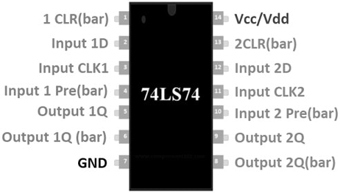
74LS74 D Flip Flop Pin Configuration
- Pins1,13 (1CLR (bar) / 2CLR (bar)): These are clear data pins of two flip flops that reset the FF by clearing simply its memory.
- Pins 2,12 (1D /2D): These are the data input pins of the two flip-flops.
- Pins 3, 11 (1CLK / 2CLK): These are CLK input pins of FFs which are provided through a CLK pulse for the FF.
- Pins 4, 10 (1PRE (bar) / 2PRE (bar)): These are PRE input pins of flip flops which are also called set pins.
- Pins 5,9 (1Q /2Q): These are output pins of two Flip Flops.
- Pin 6,8 (1Q’/ 2Q’): These are complementary outputs of Flip Flops.
- Pin7 (Vss/GND): This pin is connected to the GND terminal of the system
- PIn14 (Vcc/ Vdd): It is a voltage supply pin that supplies power to the IC normally 5Volts.
Features & Specifications:
The features and specifications of 74LS74 D Flip Flop are discussed below.
- This IC includes dual flip-flops.
- Its operating voltage ranges from 2Volts to 15Volts.
- Its propagation delay is 40nSec.
- Its min high range i/p voltage is 2Volts.
- Its max low-range i/p voltage is 0.8 volts.
- Its operating temperature ranges from 0 to 70°C.
- Its high range o/p current is 8mAmps.
- This IC includes 14 pins.
- It is available in SO-14 and SOT42 packages.
- The type of mounting is Through Hole.
- Its packaging is the tube.
- Its moisture sensitivity level is 1 (Unlimited).
- Its function is Set(Preset) & Reset.
- Its polarity is Non-Inverting.
- Its CLK frequency is 20MHz.
- Its turn-on delay time is 35 ns.
- The type of trigger is a positive edge.
- The type of CLK edge trigger is the positive edge.
- The logic function is AND.
- The equivalent 74LS74 D Flip Flop ICs are 74LVC2G80 and HEF40312B.
Working
The 74LS74 D FF IC working is simple & straightforward. This IC simply carries the Schottky TTL circuitry for producing high-speed D-type FFs. In this chip, each D-FF is available with separate inputs & complementary outputs.
When the power supply is given to the IC with the Vcc & GND pins then every flip-flop within the IC works separately. The input is given at pins 2 & 3 of the first flip-flop whereas the output can be obtained at pins 5 & 6. Here, pin 3 must be given normally with a CLK source, normally a PWM signal from a 555 timer IC or an MCU. The data & reset of this flip-flop can be cleared by making pin 3 high. The functional table of this flip-flop is shown below. The ‘X’ symbol within the table means don’t care.
|
Inputs |
Inputs | Inputs | Outputs | Outputs |
Outputs |
|
PRE (bar) |
CLR (bar) | CLK | D | Q | Q’ |
|
L |
H | X | X | H | L |
| H | L | X | X | L |
H |
|
L |
L | X | X | H | H |
| H | H | – | H | H |
L |
| H | H | – | L | L |
H |
| H | H | L | X | Q0 |
Q0 (bar) |
Clap Switch using 74LS74 D Flip Flop
This simple clap switch circuit with 74LS74 D Flip Flop is shown below. This circuit load can be turned ON/OFF through the human hand clap. The clap sound intensity is identified by a microphone which includes a diaphragm. Whenever the sound of a human clap strikes the diaphragm, then it vibrates as well as modifies the capacitance. Once the capacitance is changed then the voltage can also be changed. So this simple circuit is extremely suitable for beginners. In this circuit, the energy created can be understood through sound vibration.
The required components to make this circuit mainly include IC 7474 Dual D flip flop, IC 555, 5V Relay, Condenser Mic, BC547 Transistors, LED, 1N4007 diode, capacitors like 10 μF & 0.01 μF, resistors like 47KΩ, 1KΩ -2, 100KΩ, 9V battery and two pin connector.
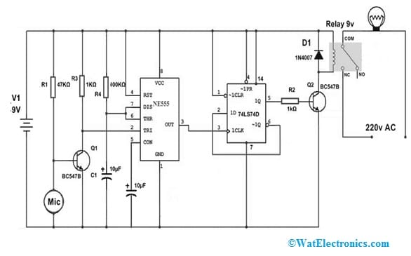
Clap Switch using 74LS74 D Flip Flop
Working
The above clap switch circuit includes three stages; The first stage is a sound detector stage which can be formed with a BC547 transistor as well as a condenser mic. The second stage includes a NE555 timer IC where this IC is used as a monostable multivibrator. So it produces a timing pulse based on the R3 timing resistor & C1 capacitor respectively. The output of this timer IC is given to the third stage which includes a 74LS74 D Flip Flop.
The input pulse from the timer IC is used to drive the D FF into either reset or set. After that, the relay is connected at the o/p of the D FF. In the set condition of flip flop, the relay will be activated and turns ON the load within the set condition whereas in reset condition, the load will be turned OFF.
This circuit is applicable in speed recognition equipment, Hearing aid devices, electronic gadgets sensitive to sound, automation systems used in industrial or home and tape recorders, etc.
Applications
The applications of 74LS74 D Flip Flop are discussed below.
- 74LS74 D Flip Flop is used in different latching instrument categories.
- In buffer circuits, this FF is a significant component.
- These FF ICs are used in TVs, memory units, etc.
- These are used in PCs, notebooks, digital electronics & networking devices.
- These D FF ICs are used in buffer & sampling circuits.
- These can be used as memory/control registers or shift registers.
Please refer to this link for the CD4014 Shift Register.
Please refer to this link for the 74LS74 D Flip Flop Datasheet.
Thus, this is an overview of 74LS74 D Flip Flop, pin configuration, specifications, circuit, and its applications. The other D Flip Flop ICs are also available in the market which are used based on the requirement like; SN74F74N, 74LVC2G80, HEF4013BP, etc. Here is a question for you, what is JK Flip Flop?