A step-down switching regulator can also be known as a DC-DC step-down regulator or buck converter device. These are a subclass of voltage regulators that decrease the voltage from an i/p to an o/p. This regulator uses a switch to separate a DC voltage and, after that uses a capacitor and an inductor to smooth the results. These regulators achieve impressive efficiencies of up to 96% and fit seamlessly into small circuits. Engineers use them in battery-operated devices to optimize battery life effectively. Step-down switching regulators maintain a stable output voltage for an electronic circuit. MAX639 IC’s are significant for the secure operation of electronics. Examples of step-down switching regulators are; MAX640, MAX653, MAX639, etc. This article overviews what is MAX639 IC, its pin-out, features, specifications, and applications.
What is MAX639 IC?
MAX639 is a series fixed or adjustable output and step-down switching regulator. The input voltage of this voltage regulator ranges from 5.5 to 11.5V, the output voltage is +5V & output current is about 100mA. This step-down switching voltage regulator provides high efficiency over a broad range of load currents to deliver up to 225mA current. The MAX639 voltage regulator has a 1A power MOSFET switch internally which makes it perfect for minimum-component, medium-power, and low-power-based applications. This step-down controller increases output driveability to drive an exterior P-channel FET mainly to deliver equal to 5W.
Working
The MAX639 step-down switching voltage regulator works with a current-limiting PFM (pulse-frequency-modulated) control method. Thus, this allows the MAX639 IC to be extremely efficient over an extensive range of load currents while utilizing 10µA of current supply only. Its outcome is highly efficient above a wide range of loads. The MAX639 IC is a high-efficiency, low-power, and step-down DC-to-DCC converter that provides 5V regulated output for up to 225mA load currents.
MAX639 IC Pin Configuration:
The pin configuration of MAX639 IC is shown below.
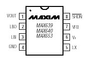
MAX639 IC Pin Configuration
- Pin-1 (Vout): It is an output voltage pin of the IC.
- Pin-2 (LBO): It is a low battery output of regulator IC.
- Pin-3 (LBI): It is a low battery input pin.
- Pin-4 (GND): It is a ground terminal of IC.
- Pin-5 (Lx): It is a MOSFET Drain pin of the regulator.
- Pin-6 (V+): It is a positive voltage supply pin of the voltage regulator IC.
- Pin-7 (Vfb): It is the voltage feedback pin of the IC.
- Pin-8 (SHDN): It is a shutdown pin of the voltage regulator.
Key Features
- Step-Down Switching Regulator: Operates in buck topology to efficiently convert higher input voltages to stable lower output levels.
- Compact 8-Pin Package: Available in SOIC-Narrow-8, suitable for space-constrained designs.
- High Efficiency: Maintains efficiency of over 90% across a wide load range.
- Low Quiescent Current: Consumes only 10 µA, making it ideal for portable and battery-operated devices.
- Integrated MOSFET Switch: Includes a 1A internal power MOSFET, allowing direct drive capability with fewer external components.
- Current-Limiting PFM Control: Uses Pulse-Frequency Modulation (PFM) for efficient power management and stable regulation.
- Low-Battery Detection: Features an onboard comparator for monitoring battery voltage and providing low-battery warnings.
- Shutdown Mode: A dedicated SHDN pin allows power-saving shutdown control.
Electrical Specifications
- Input Voltage Range: 4 V to 11.5 V.
- Fixed Output Voltage: +5 V (adjustable output also possible with external feedback).
- Output Current Capability: Up to 225 mA.
- Output Power: Can deliver up to 5 W when driving an external P-channel FET.
- Number of Outputs: Single output.
- Quiescent Current: 10 µA (typical).
- Operating Temperature Range: 0 °C to +70 °C.
- Mounting Style: SMD/SMT.
- Packaging: Reel for automated PCB assembly.
Equivalents & Other ICs
Equivalent MAX639 ICs are; MAX65, MAX640, etc. Alternative step-down switching regulators are; MP1584, LM2679, LM2596, MP4560DN, HTC LM2596R, etc.
Comparison of MAX639 vs LM2596 vs MP1584
| Parameter | MAX639 | LM2596 | MP1584 |
| Type | Step-Down Switching Regulator (Buck) | Step-Down Switching Regulator (Buck) | Step-Down Switching Regulator (Buck) |
| Input Voltage Range | 4 V – 11.5 V | 4.5 V – 40 V | 4.5 V – 28 V |
| Output Voltage | Fixed 5 V (adjustable with feedback) | Fixed 3.3 V, 5 V, 12 V or adjustable | Adjustable: 0.8 V – 25 V |
| Output Current | Up to 225 mA (5 W with ext. P-FET) | Up to 3 A | Up to 3 A |
| Efficiency | Up to 90–96% | ~73–90% | Up to 95% |
| Switching Frequency | Pulse-Frequency Modulation (PFM) | ~150 kHz | ~1.5 MHz |
| Quiescent Current | 10 µA | ~5 mA | ~1.2 mA |
| Internal Switch | 1A Power MOSFET | Internal Power MOSFET | Internal Power MOSFET |
| Special Features | Ultra-low power, Low-battery detection | Simple, widely used, robust | Compact, high-frequency, small footprint |
| Package Options | SOIC-8 | TO-220, TO-263, D²PAK | SOIC-8, QFN |
| Applications | Portable devices, low-power circuits, NiCad battery chargers | General-purpose DC-DC regulation, Arduino, LED drivers | Compact power supplies, drones, IoT devices, telecom |
Solar Nickel-Cadmium NiCad Battery Charger Circuit with MAX639 IC
The solar NiCad battery charger circuit is mainly designed for low-power (or) low-ampere-hour NiCad battery chargers. This circuit uses up to 12 solar cells to charge the NiCad battery. This simple circuit uses a voltage regulator to ensure a stable charging voltage mainly for the battery. In addition, this circuit charges small NiCad batteries efficiently without disturbing damage or overcharging.
The required components to make this circuit mainly include; resistors like 820k, two 75k and 1M, capacitors like 16V,47uF, 40V,100uF, MAX639 IC, 1N57117 Zener diodes, and 100uH coil inductor. Connect this circuit as per the diagram shown below.
MAX639 switching regulator IC is utilized to step down voltage and provides 200mA output current in a secure range. This circuit has a very high efficiency because of the function of pulse frequency modulation. The Input voltage range of MAX639 is 4V to12V and can provide o/p voltage from 1.5V to the highest input voltage.
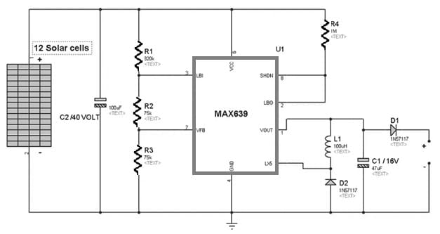
Solar Nickel-Cadmium NiCad Battery Charger Circuit
Working
The solar panel in this circuit plays a key role in changing the sunlight into electrical energy. Here, the number of solar cells utilized mainly depends on the preferred charging current and the battery capacity you desire to charge. But this circuit uses 12 solar cells, even though you can change this number based on your requirements.
The solar panel in this circuit can be connected to a current-limiting resistor & a diode. Here the main function of the resistor is to limit the charging current supplied into the battery, preventing it from surpassing the suggested value. The diode in this circuit allows current in one direction only.
Here batteries charging current should not go beyond 200mA to avoid overcharging. A voltage regulator is used to change the voltage & current. Therefore, this voltage regulator maintains a stable output voltage irrespective of variations within the input voltage (or) load conditions. So it provides a constant charging voltage mainly for the battery for best charging performance.
This circuit is designed especially for low-power applications & smaller NiCad batteries. This circuit’s overall performance can change based on various factors like the intensity of sunlight, battery conditions, and weather conditions. This circuit can provide a reliable & sustainable solution for small NiCad batteries charging with solar energy by following the right security measures and checking the charging process.
Compact Step-Down Switching Converter with MAX639 IC
SMPS is commonly used in electronic circuits to step up or down voltage levels efficiently. SMPS generate minimum heat which leads to high efficiency. This efficiency will be helpful mainly for compact power supplies because it eliminates the requirement of forced-air cooling. Designing a switch-mode supply with an MAX639 step-down converter is much simpler.
The required components to make this circuit include MAX639 IC, 1N5817 Diodes, 100µ 16v capacitors, 10kΩ and 10MΩ resistors. Connect this circuit as per the circuit shown below.
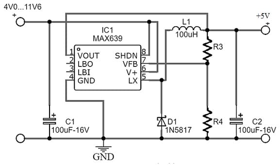
Compact Step-Down Switching Converter with MAX639 IC
Working
If we design a compact electronic device then that needs to change a higher input voltage to a constant +5V output, however, space and efficiency are significant. Linear voltage regulators won’t function because of inefficiency and extreme generation of heat. Engineers incorporate the MAX639 step-down converter to achieve high efficiency and minimize heat generation, making it ideal for compact designs.
The input voltage of this circuit ranges from 4V to 11 V, and the output voltage it produces is +5v (or) adjustable. With an output current of 100mA and a conversion efficiency exceeding 90%, this converter effectively detects low-voltage batteries and controls ON/OFF modes.
The MAX639 integrated step-down converter IC is a highly efficient and solid solution mainly for voltage regulation within electronic circuits. This circuit not only reduces heat generation but also simplifies the design process, making it perfect for applications where space and cooling options are limited.. It provides reliable performance across various devices & projects.
Advantages & Disadvantages
The advantages of MAX639 IC include the following.
- The MAX639 step-down switching regulator t is highly efficient over a large range of load currents.
- It uses 10µA of current supply only.
- This IC has an internal 1Amps power MOSFET switch which makes it perfect to use in low to medium-power-based applications.
- Users can adjust the output voltage of the MAX639 IC to any level between 1.3 volts and the input voltage
- It is an efficient, low-power, multi-functional, low-dropout switching regulator.
The disadvantages of MAX639 IC include the following.
- Electromagnetic interference should not trouble near the regulator IC or circuitry.
- These regulators change fairly small energy into heat.
- The possible interferences on the supply can occur because of the burst mode as well as the exorbitant price.
- These regulators are complex ICs that need more exterior parts like resistors, capacitors, transistors, and diodes. Thus, this makes them more hard to design and obtain working properly.
- The high-frequency switching of these regulators can produce huge noise with current and voltage ripple at the I/O filters.
- The level of incorporation within switching regulators can be costly, and the IC size can enlarge.
Applications
The applications of MAX639 IC include the following.
- The MAX639 voltage regulator converts 5Volts to 3.3Volts, (or) a 9V battery to 5Volts, 3.3Volts (or) 3V supply.
- These regulators replace high-efficiency linear regulators
- It can be utilized in handy terminals and portable instruments.
- In addition, the MAX639/MAX640/MAX653 have an internal 1A power MOSFET switch, making them ideal for minimum-component, low- and medium-power applications.
- The MAX639 step-down converter IC is a compact and highly efficient solution mainly for voltage regulation within electronic circuits.
- This IC drives an exterior P-channel FET to deliver a 5W supply for improved output driveability.
Please refer to this link for the MAX639 IC Datasheet.
Thus, this is an overview of MAX639 IC, pinout, features, specifications, circuit, working, and applications. The MAX639 power management IC is a basic building block in modern electronic devices that can function as oscillators, amplifiers, counters, timers, computer memory, logic gates, microprocessors, microcontrollers, etc. This is an efficient, low-power, and step-down DC to DC converter IC which provides a 5V regulated output for up to 225mA load currents. Here is a question for you, what is LM2596 IC?