In this digital world of electronics, the information is stored in the form of bits (Binary). Certain arithmetical operations like addition, subtraction, multiplication, and division are to be performed on these bits. The combination of ‘Arithmetic Operation’ with certain ‘logic’ using binary numbers was established by Leibniz. Further, the electrical circuits of switching based on vacuum tubes were designed. The invention of relays replaced the ‘vacuum tubes’ in switching circuits. Finally, all the inventions lead to the destination of the logic gate.
As there were step-by-step revolutions in digital electronics, Konrad Zuse is the man who was behind the development and the design of ‘Electrochemical Logic Gate’. The ‘Boolean Algebra’ and the switching operation from then on were carried out by the logic gates. Let now get into detail about how are these logic gates designed and their different available types.
Table of Contents
- What is Logic Gate?
- Types of Logic Gates
-
- AND
- OR
- NOT
- NAND
- NOR
- XOR
- X NOR
3. Uses of Logic Gates
4. FAQ’s
What is Logic Gate?
A digital electronic circuit that is made to perform certain logical operations is defined as Logic Gate. It can be designed using any ‘Non-Linear Device’. The sole condition is that it must consist of two different regions for operation.
The most commonly known devices with non-linear characteristics are Diode and the Bipolar Junction Transistors (BJT). The logic levels of voltages are assigned to the circuits to carry out the operation. The logic assignment of supply voltages can be of two types. It can be classified as a Positive Logic System and a Negative Logic System. In the positive system, logic 1 is +5 Volts and logic o is 0 volts. The level assignment is reversed in the negative logic system. The most commonly preferred system is Positive Logic.
The most common example of an assignment of the logic level is ‘Light Bulb’. It gets switch ON or OFF based on logic 1 and logic 0 applied.
Types of Logic Gates
The design of digital circuits is based on logic gates. The combination of input signals is applied to generate a single output. Initially, there are three basic logic gates. They are AND, OR, and NOT.
The output generation is based on the type of input bits applied. For instance, if input 11 is applied for the AND gate the output is 1 and for the NAND gate, it will be 0. Similarly, the values differ based on the type of logic gate chosen.
AND Gate
It consists of ‘two or more inputs and produces only one output. If each of the inputs applied to the gate is logic 1 then the output will be logic 1. Otherwise, if any one of the inputs is 0 the output generated will be 0. This type of functionality gate is defined as an AND gate. The AND gate is also known as the ‘ALL’ or ‘NOTHING’ gate.
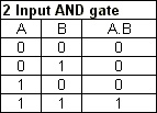
AND Gate Truth Table
If the inputs applied are A, B. Then the output ‘Z’ generated can be expressed as Z= AB.
The symbol for AND Gate is
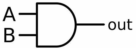
AND Gate Symbol
The realization of AND gates is also done by using Transistors and Diodes. When the two diodes are connected along with a resistor and based on the supply provided the output is generated.
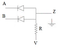
AND Gate Realization using Diodes
when both A and B are applied with +5 Volts. The diodes remain OFF. Hence there is no chance of occurrence of Voltage Drop across the resistor. Therefore the output obtained is high. When both the input values are provided with 0 Volts the circuit will be short-circuited. Practically o volts are not possible it refers to 0.6 or 0.5 volts.
The circuit of AND can also be realized by using transistors. When both the inputs or even any one of the output is o then the base current drives the Q3 to ON. Therefore, the output obtained because of Q3 is 0 volts.
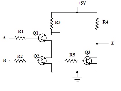
AND Gate (Using Transistors)
When both the inputs are +5Volts both Q1 and Q2 are ON. Hence no base current can drive the transistor Q3. Therefore Q3 is OFF and the output obtained is +5Volts.
OR Gate
Likewise, the AND gate the OR gate has two or more inputs and one output. The output of the OR gate is high if both the inputs are high or even one of the inputs is high.
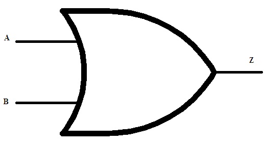
OR Logic Gate
The Truth table of OR clearly states that the value of output remains high even if the single output is high. If the inputs applied are A and B and the output obtained is denoted by Z.
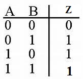
OR Truth Table
The same circuit realization can be done based on diodes. To the applied inputs the diode behaves accordingly. When both the applied inputs are 0 volts then diodes remain OFF. Then no chance of current flow through the circuit. Hence there is no voltage drop crossover in the resistor. Therefore the output generated is 0 volts.
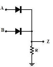
Logic Gate OR
If anyone of the input or both the inputs applied are high. Then both the diodes or either of the diode is high the current flows through the circuit. The output generated due to this is high. Similarly, the same operation of OR is realized using transistors in the circuit.
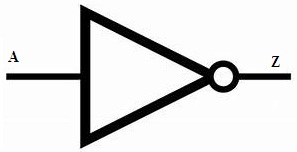
NOT Gate
Last but not least in the category of basic gates is the NOT gate. Generally, it consists of one input and one output. If the value applied at the input is 1 the output will be 0 and vice-versa.
The symbol for the logic NOT gate is
Logic Gate NOT
The Truth Table for the NOT gate is
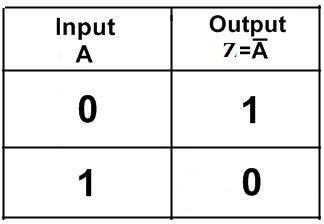
Truth Table Not Gate
NAND Gate
The combination of AND and NOT gates connected in series is defined as the NAND gate. All types of binary operations are performed by these gates.
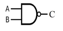
NAND Gate Symbol
The Truth Tabe of the NAND gate is
Truth Table of NAND Gate
When both the inputs applied are 1 the output obtained is 0. The operation of the NAND gate can be understood based on the circuit diagram and the applied inputs.
Logic Circuit Diagram (NAND Gate)
As per the above circuit connection between diodes and an NPN transistor the circuit for the NAND gate is designed. It is the combination of AND gate followed by an inverter. If both the inputs that are A and B applied with 1 both the diodes are reverse biased. Then the overall supply reaches the base of the transistor Q1. This turns the transistor ON and the voltage gets short-circuited to the ground. Hence the output obtained becomes zero.
Similarly, the diodes are forward biased for the other applied inputs and the transistor is in OFF mode. Therefore the outputs obtained in such cases are high.
Please refer to this link to know more about NAND Gate MCQs
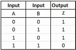
NOR Gate
The combination of an OR gate followed by an inverter is determined as the NOR gate. The reverse operation of the OR gate is observed in the NOR gate. In the OR gate, the outputs are high if any one of the inputs or both the inputs is high. But in this gate, the output is high if both the inputs are 0 or LOW.
The symbolic representation of the NOR gate is
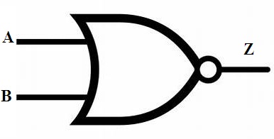
Logic Symbol of NOR Gate
The Truth table for this gate is
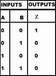
NOR Gate Truth Table
This type of gate generates output as high when both the inputs are 0 volts.
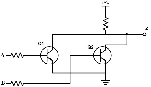
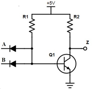
Logic Circuit Diagram of NOR Gate
When both the inputs applied are of 0 volts both the transistors Q1 and Q2 are OFF. Hence there is no voltage drop developed across the resistor. The final output generated is of +5 volts. For the other applied input, either one of the transistors will be ON or both the transistors are ON. In this situation, a certain voltage drop is generated. This produces low levels of output.
XOR
Two inputs applied to the gate to generate a single output which is capable of producing logic 1 as output when any one of the inputs is high. The purpose of this gate is to detect inequality. This is also referred to as ‘Inequality Detector’. By the connection of logic 1 to any of the input terminals, the circuit behaves as an inverter.
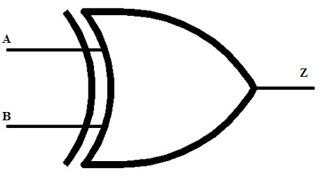
Logic Gate XOR
The Truth Tabe for this XOR gate is
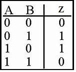
Truth Table of XOR Gate
From the truth table, it can be intelligibly stated that for the applied odd inputs of 1 the resultant will be logic 1. If more than two inputs are considered then the behavior of this gate is decided based on its implementation. The operation performed by XOR is excluding the carry bit. This is the reason for defining this gate as an Exclusive OR gate.
The Boolean Expression to define the operation of the XOR gate is
Z= A⊕B
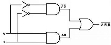
The logic circuit diagram for this exclusive gate is designed in the combination of AND and OR gates at the output.
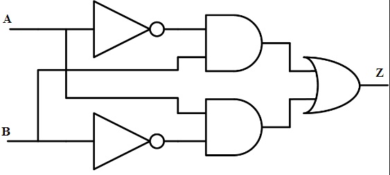
Logic Circuit Diagram of XOR Gate
Please refer to this link to know more about XOR gate MCQs.
XNOR
The combination of the XOR gate with the basic NOT gate results in the formation of the XNOR gate.
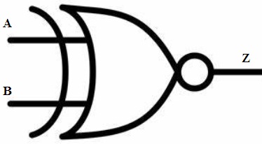
Logic Symbol (X NOR Gate)
The reverse operation of XOR is performed in X NOR. When both the inputs are o or if both the inputs are 1 the resultant is logic 1 otherwise logic 0 for further inputs.
The truth table for the gate is
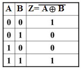
Truth Table of X NOR Gate
The logic circuit diagram for this kind of operation is
Logic Circuit Diagram of X NOR Gate
Please refer to this link to know more about XNOR Gate MCQs.
Uses of Logic Gates
Logic gates are the essentials for the designing of digital circuits. Some of them are described as follows:
- In the design of the combinational circuits called Demultiplexers, Multiplexers, and other digital circuits, these gates are used.
- The detection of the number of events that took place in any situation can be estimated using these gates in the circuits.
- In certain cases of generation and checking of parity bits, these gates are used.
Please refer to this link to know more Combinational Logic Circuits MCQs & Logic Gates MCQs
FAQ’s
1. Who invented Logic Gates?
Konrad Zuse is the man behind the basic design of logic gates.
2. What is the Principle of Logic Gates?
The logic gate works on the principle of discrete connection of non-linear devices. For example, the combination of transistors is connected to form the logic gates.
3. What are the three basic Logic Gates?
The three basic logic gates are AND, OR, and NOT.
4. What are the seven Logic Gates?
The seven logic gates are AND, OR, NOT, NAND, NOR, XOR, and X NOR.
After the overview of all the basic logic gates. One can predict the importance of it in digital circuits. Can you determine what is the most preferred IC for such arithmetic operations?