Binary Adder and Subtraction Circuits are known for the operations that are used in digital computations. There are various processes performed by the digital circuits among which arithmetic operations are prominent. The operations can be successfully implemented by using ‘Logic Gates’. There are various gates such as AND, OR, NOT and NAND,exclusive OR etc… among all those exclusive OR is preferred for the addition of binary values.
There is a basic difference between the Inclusive type of OR gate and the Exclusive type. The inclusive is known for the addition of the integers. For the binary arithmetic operations, exclusive OR gates are preferred.
What is a Binary Adder?
The adder that performs the addition of the binary values and generates the sum in the same format can be referred to as Binary Adders. These types of circuits are utilized in the calculators, computers for ALU units, etc…
Binary Addition Circuits
The basic arithmetic operations are additions and subtractions of the binary digits. The simplest operations of additions are
- 0+0= 0
- 0+1=1
- 1+0=1
- 1+1= 10
The sum value produced by the above operations produces the value of the single-digit . But in the case where both the bits are present, that is ’11’ a carry is generated. The first term used besides is known as augends and the second term is known as an addend.
The operation performed is dependent upon the number of bits. If the addition of two bits is to be done then half adder is preferred. If it is about three bits then the full adder circuit is preferred.
-
Half Adder
This the circuit is of combinational type. The two inputs of binary are applied for which it results in two binary outputs. When the addition of inputs takes place the resultant generates a ‘Sum’ and the ‘Carry’.
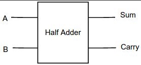
Half Adder Block Diagram
The circuit with logic gates and the truth table of this circuit is as follows;
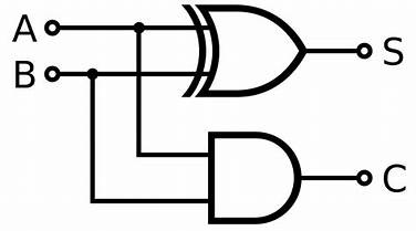
Half Adder Circuit
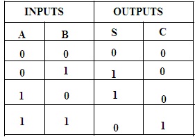
Half Adder Truth Table
-
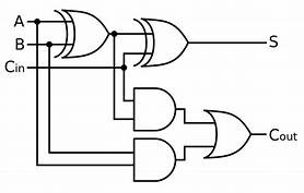
Full Adder
The half adder circuit can only add two numbers. If it is required to considered the carry bit for the next sequence of addition then in that case the half adder circuit will not work. In this scenario, we go in for a full adder circuit which takes in the three inputs. Among those three the two bits results in sum and the third bit is for carrybit from the previous addition . At the outputs two bits are obtained which is the sum and the carryout. The addition of the bits initiates from LSB. If the carry is generated in the first LSB bits then it will be passed further.
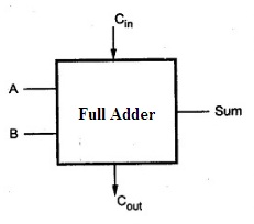
Full Adder Block Diagram
The circuit diagram and the truth table of this circuit are as follows:
Full Adder Circuit Diagram
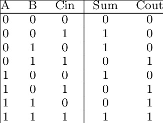
Full Adder Truth Table
Binary Subtraction Circuits
The subtraction is not just as simple as an addition. When the two bits of these numbers have used the complement of the value at ‘subtrahend’ must be added to the ‘minuend’. Hence by taking the complement of the number instead of subtraction we need to add the value.
Therefore the method of the subtraction can be converted into addition. There is no necessity for special circuits in such cases. Even the adder circuit is sufficient for subtraction. Like half and full adders, there are circuits for subtraction known as half subtractors and full subtractors.
This is also a combinational type of circuit. It possesses multiple outputs. Initially, two digits of input applied to generate two values of outputs that are difference bit and the borrow bit. This process of operation can be carried out by the XOR gate including the AND gate as an additional one. Where the value of the input is complemented by NOT gate before given to AND gate.
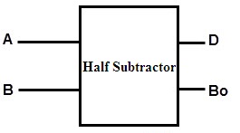
Half Subtractor Block Diagram
The circuit diagram for the half subtractors and the truth table is
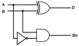
Half Subtractor Circuit
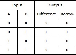
Half Subtractor Truth Table
2.Full Subtractor
Full Subtractor performs the subtraction process which involves three bits of input that generates two bits as output. Among those three digits, two are preferable digits for subtraction and the other digit, borrow generated from the previous operation.
The circuit representation and its truth table can be described as
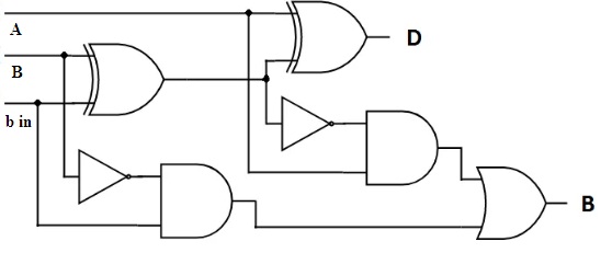
Full Subtractor Circuit
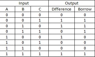
Full Subtractor Truth Table
Parallel Binary Adder
The parallel circuit for the addition of the binary values can be obtained by establishing a connection between the ‘Full Adders’. The connection is possible by connecting the output carries as the input to the other adders. Based on the number of bits number of full adders is connected.
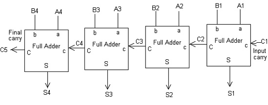
Parallel Adder
These circuits of adders are enclosed in the form of IC’s. These are designed such that it must have terminals of four augends and terminals for the adding the bits. The two numbers can be added simultaneously in these circuits. But there is no value of carrying at the least position. In these adders, the primary block is half adder followed by full adders.
Parallel Binary Subtractor
The parallel type of Binary Subtractor can be designed with 4 bits. Let us consider A-B. In this case to perform subtraction one has to take two’s Complement of B. then that complemented value should be added to A.
The two’s complement can be carried out by taking the one’s complement of the number then by adding the value 1 to the least significant bit of the complemented value. There are various ways through which these subtractors are designed. Even the combination of half and full subtractors can be used for the design of these subtractors.
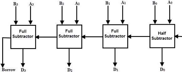
Parallel Subtractor
The bit values ‘A3A2A1A0’ known as Minuends in the circuits are subtracted by the Subtrahend of ‘B3B2B1B0’. The borrow generated can be connected further as the input value for the preceding subtraction unit.
Binary Adder-Subtractor
In this case, both the arithmetic operations called addition and subtraction are performed in one circuit. This is possible by using the logic gate called X-OR. There is a mode control provided which decides it must be an adder or a subtractor. When M value is 0 the circuit performs the addition operation. If M=1 then the circuit performs subtraction.
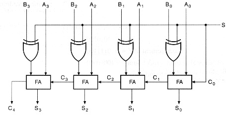
Binary Adder or Subtractor
Each of the XOR gate used in the circuit consists of two input connections. Among those two inputs, one is for M and the other is for B. as the S value is maintained 0 B XOR of 0= B. Then the circuit performs the task of addition. When S =1 the circuit produces B XOR of 0 = Complement of B. Then the value that is complemented is added to A. This kind of operation is also referred to as two’s complement. Hence the two arithmetic operations are performed in a single circuit.
Please refer to this link to know more about Binary Addition MCQs & Binary Subtraction MCQs.
Practically in the process of addition and subtraction can be performed by these circuits in computers, the devices where the micro controller is the basic units and the digital calculators. These are also preferred in networking as well as the Digital Processing of the Signals. We have discussed the parallel adder above. In that process, the carry has been forwarded to the next stage. If in certain stage carry is not generated the circuit generates time delay. To overcome another adder circuitry is designed. Can you identify which circuit can overcome the delay in the addition operations?