A signal generator is a device that generates repeating or non-repeating signals to test and estimate electronic systems. The main function of a signal generator is to simulate real-world conditions & signals by allowing designers to test the circuits & equipment’s performance. These signal generators can generate frequencies from 500 Hz to 1.5 MHz. These generators can come in different sizes and shapes, from handheld device models to benchtop models. These are used for circuit testing, design verification, component characterization, radar technology development, audio system fine-tuning, etc. Thus, this article elaborates on the AD9850 DDS signal generator, pinout, specifications, and applications.
What is the AD9850 DDS Signal Generator?
AD9850 is a DDS (Direct Digital Synthesizer) signal generator, a small and very affordable board that generates analog signals used in small-signal generation projects. This module is available in a 28-lead SSOP or surface-mount space-saving package.
This highly integrated chip leverages advanced DDS technology, featuring high performance, a high-speed comparator, and a D/A converter to create a digitally programmable frequency synthesizer and clock generator. Thus, DDS technology is a technique that generates a sine wave, usually known as an analog waveform, by producing a time-varying signal within digital form. After that, it performs a DAC (digital-to-analog conversion).
The innovative high-speed-based DDS core of this module provides a 32-bit frequency tuning word, thus resulting in 0.0291 Hz output tuning resolution for a 125 MHz reference CLK input. The frequency tuning, phase modulation, and control words are loaded simply into the module through a serial loading or a parallel byte format.
DDS Flow:
The AD9850 DDS signal generator processes a digital frequency tuning word to create an analog output signal through a phase accumulator, sine lookup table, and a DAC (digital-to-analog converter). The DDs flow is: first, a digital tuning word is fed into a phase accumulator to generate an equivalent phase value. This phase value is used as an index into a sine lookup table, which stores digital value that represents the sine wave amplitude at different phases. After that, the digital value can be converted to an analog voltage from the lookup table using the DAC, and provides the analog sine wave output.
The complete DDS of AD9850 utilizes very advanced CMOS technology to give this breakthrough level of performance and functionality on 155 mW of power dissipation only. Particularly, digitally programming the AD9850 module with DDS technology (or) a microcontroller helps control movements. So, a DDS frequency synthesizer produces signals or waves that can be viewed from an oscilloscope.
AD9850 Components
The AD9850 AD9850 DDS signal generator module includes different components like a crystal Oscillator, Duty Cycle or Amplitude Adjustment, AD9850 IC, and Power LED, which are discussed below.
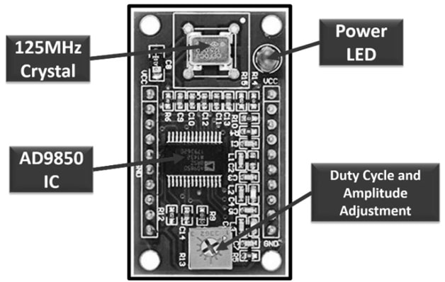
AD9850 Components
- The crystal oscillator module includes a crystal oscillator, which provides CLK & timing control mainly for the IC.
- The duty cycle (or) amplitude adjustment of the module adjusts the offset and pulse widths of the signal through the integral potentiometer.
- AD9850 IC in this module is used to process all the tasks using a powerful oscillator & other components, and it outputs analog signals.
- The power LED in this module indicates the condition of the power supply.
Working
The AD9850 module employs DDS (direct digital synthesis) technology to generate an analog sine wave output that you can program for both phase and frequency. It features a 125 MHz active crystal oscillator, which produces a highly precise pulse source.
This allows you to digitally modify the output frequency at speeds of up to 23 million changes per second. You can easily set the output frequency by loading a 40-bit tuning word into the direct digital synthesis, which consists of 32 bits for frequency and phase data, along with 8 bits to configure the operating modes of the DDS.
Additionally, you can use this module as a frequency source or convert it to a square wave for use as a clock generator. So the output wave produces two sine waves or two square waves. This module includes a 125 MHz CLK rate, a high-speed comparator, and a high-performance DAC.
AD9850 DDS Signal Generator Pin Configuration:
The pin configuration of the AD9850 DDS signal generator is shown below. This module includes different pins, which are discussed below.
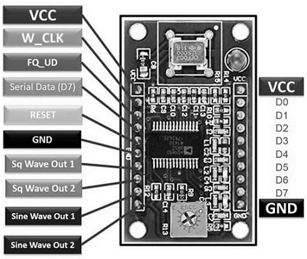
AD9850 DDS Signal Generator PinOut
- Pin (VCC): This is a voltage supply pin that provides 3.3V or 5V input power to the module.
- Pin (GND): It is the ground pin of the module.
- Pin (W_CLK): It is the word load CLK pin of a module. So the DDS updates the frequency or phase loaded within the data input when the clock edge increases.
- Pin (DATA): It is a data pin where serial input data can be supplied throughout the D7 pin.
- Pin (RST): This is the master RST function of the module. Whenever this pin is set too high, it clears all registers apart from the input register. So the output of DAC goes to Cosine 0 after extra clock cycles.
- Pins (D0–D7): These are 8-bit serial data input pins of the module.
- Pin (Square Wave Output 1): This is the accurate output pin of the comparator.
- Pin (Square Wave Output 2): This is the complement output of the comparator.
- Pin (Sine Wave Output 1): It is an analog current o/p pin of the DAC.
- Pin (Sine Wave Output 2): It is the complementary analog o/p pin of the DAC.
Features & Specifications:
The features and specifications of the AD9850 DDS signal generator include the following.
- AD9850 is a signal generator module.
- Its operating voltage supply range is from 3.3V – 5V.
- Its output frequency range is from 0 to 40 MHz.
- Its continuous digital output current is 0.005A.
- DAC output current is 0.03A.
- Its storage temperature ranges from -40~ +80°C
- Its operating temperature ranges from -40~ +85°C.
- This module’s dimensions L×W*H are 50*30*20mm.
- Its oscillator frequency is 125 MHz.
- Power dissipation is 380 mW at 125 MHz, 5V.
- Power dissipation at 110 MHz, 3.3V is 110 mW.
- Data transmission can be either serial or parallel.
- It includes a power-down function mainly for a short boot time.
- Power dissipation mainly depends on the voltage supply.
- DDS mainly depends on CMOS Technology, it provides better functionality and performance.
- It has four analog signal outputs like sine-wave-1, sine-wave-2, square-wave-1 & square-wave-2.
Equivalents & Alternatives
The equivalent AD9850 DDS signal generators are: AD9851, ICL8038, etc. Its alternative AD9850 DDS signal generators are; AD9833, AD9830, AD9831, AD9834, AD9832, AD9958, AD9959, AD9106, AD9838, AD9835, etc.
AD9850 DDS Signal Generator Interfacing with Arduino Board
AD9850 module interfacing with the Arduino Board is shown below. So, a signal generator is an electronic device that creates both repeating & non-repeating analog or digital signals. Thus, this AD9850 module generates a DDS (Direct Digital Signal). This function generator is a tiny-sized module that generates output waves at 0 to 40 MHz frequency, including two sine waves and two square wave o/ps.
The AD9850 DDS signal generator module has a DSS synthesizer, a timing control used for the IC & 125MHz oscillator to provide CLK. This module is equipped with a potentiometer internally that can modify the pulse lengths & the signals’ offset.
The required components to make this interfacing mainly include Arduino Uno, a Type A to B USB Cable, AD9850 DDS signal generator module, and jumper wires. So the connections of this interfacing follow as;
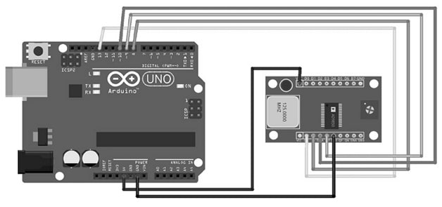
AD9850 Module Interfacing with Arduino Board
- Connect the +5V pin of the Arduino board to the Vcc pin of the AD9850 module.
- Connect the D13 pin of the Arduino board to the W_CLK pin of the AD9850 module.
- The D8 pin of the Arduino board is connected to the FQ_UD pin of the AD9850 module.
- Connect the D10 pin of the Arduino board to the Data pin of the AD9850 module.
- Use the D9 pin of the Arduino board to connect to the Reset pin of the AD9850 module.
- Finally, connect the GND pin of the Arduino board to the GND pin of the AD9850 module.
Code
The required code for this interfacing includes the following.
#include <AD9850SPI.h>
#include <SPI.h>
const int W_CLK_PIN = 13, FQ_UD_PIN = 8;
const int RESET_PIN = 9;
double freq = 10000000;
double trimFreq = 124999500;
int phase = 0;
void setup(){
DDS.begin(W_CLK_PIN, FQ_UD_PIN, RESET_PIN);
DDS.calibrate(trimFreq);
}
void loop(){
DDS.setfreq(freq, phase);
delay(10000);
DDS.down();
delay(3000);
DDS.up();
delay(2000);
DDS.setfreq(freq + 500, phase);
delay(5000);
DDS.down();
while(1);
}
Working
To begin the AD9850 module within the Arduino IDE, we should install a library. This library can be installed by starting the Arduino IDE.
Navigate to Tools >Manage Libraries. After that, search for the AD9850 IC within the search bar. Select AD9850 SPI from the options, and push the install button.
Now the libraries need to be included in the code. So here we included two libraries, where one is installed & the other library is the SPI library used for communication. By using the SPI library, we can interface with a minimum of one or above SPI devices.
After that, we define the Arduino pins to which the signal generator module is connected. So we make two objects, freq & timeFreq, that store the double value.
Know that Arduino doubles have an 8-byte size. After that, we define the object phase, which initially holds the 0 value of an integer.
We initialize the module in the void setup with the DDS.begin function. This function helps to adjust the module.
After that, there is a void loop that sets up the frequencies to produce the signal.
Thus, the AD9850 module interfacing with Arduino is very simple. It requires three pins, RESET pins, W
CLK & FU UD. When the code is uploaded to the Arduino board, this module starts producing DDS signals.
Advantages & Disadvantages
The advantages of the AD9850 DDS signal generator include the following.
- The AD9850 is a highly integrated device that leverages advanced DDS technology, showcasing high performance with an internal high-speed comparator and D/A converter.
- This powerful 125 MHz CMOS DDS device is specifically designed for flexible frequency synthesis and precise clock generation.
- This module stores the waveform, which makes waveform analysis more effective.
- It measures parameters automatically like frequency, pulse width & voltage.
- This module has smart tuning that checks the speed and knob rotation duration to change the tuning speed.
- The AD9850 is a lightweight, portable, and small module.
- This module generates both square and sine waves.
- It generates sine waves with the main advantage that they can modify frequency very fast because they are based on a sine LUT & DAC.
- Officially, the AD9850 is rated for reliable sine output up to 40 MHz, while it can achieve 62.5 MHz with some degradation in quality.
- It provides 5 bits of digitally controlled phase modulation by allowing for phase shifting within increments of 11.25°, 22.5°, 45°, 90° & 180°.
The disadvantages of the AD9850 DDS signal generator include the following.
- The waveform will become less clean after 20 to 30 MHz when frequency harmonics rise.
- To ensure full access during commissioning, it’s advisable to avoid the parallel mounting arrangement.
- Using a buffer amplifier with these signal generator modules is recommended, as connecting a load can sometimes lead to unpredictable behavior.
- Additionally, be aware that these modules may experience noise and crosstalk issues.
- The software evaluation may need to have the proper port address, mainly for the parallel port.
- The sine wave’s amplitude decreases when the frequency increases
Applications
The applications of the AD9850 DDS signal generator include the following.
- The AD9850 module generates agile sine waves with phase and frequency control.
- You can use this module for clock recovery and locking circuitry, primarily in digital applications.
- It serves as a communications tool and functions as an ADC encoder generator with digital control.
- Additionally, it is suitable for local oscillator applications.
Please refer to this link for the AD9850 DDS signal generator datasheet.
Here’s a brief overview of the AD9850 DDS signal generator. This device operates on a CMOS 125MHz frequency and features a complete DDS synthesizer. It incorporates advanced DDS technology along with a high-performance, high-speed comparator and D/A converter, creating a fully digitally programmable frequency synthesizer and clock generator. The module boasts an advanced digital architecture that provides excellent control over phase and frequency, making it essential for applications ranging from amateur radio to commercial communications. Designers often choose the AD9850 module for high-performance frequency control systems due to its adaptability, reliable performance, and low power consumption. Now, let me ask you: What is the AD9833?