In digital circuits, a logic gate is a fundamental building block used to perform logical functions. At present, most of the electronic devices we use like tablets, smartphones, or memory devices have some kind of logic gates. These logic gates are also available as an integrated circuit because the single logic gate circuit which is designed manually has a very large size, so logic circuit ICs are used to solve this issue. The logic gate ICs are very small & have a very faster speed which makes them used in every kind of device. This article discusses an overview of one of the AND logic gate IC like 74LS08 AND gate IC and its applications.
What is 74LS08 AND Gate IC ?
74LS08 is a Quadruple two-input AND logic gate from the 74XXYY IC series. This logic gate IC includes four AND logic gates where each logic gate includes two inputs, thus this logic gate is called QUADRUPLE 2- Input AND logic. The gates in the chip are designed by SCHOTTKY TRANSISTORS for high-speed logic operations. The 74LS08 IC is a quadruple two-input AND logic gate IC. An AND logic gate is a type of digital circuit used to change one logic state to another.
Initially, we have to understand about AND logic gate and also its main function. AND logic gate is a significant gate used in digital logic circuits. This logic gate includes two inputs and one output. The function of this logic gate follows as; whenever any of the logic gate’s input states is zero or low, then the output of this gate is low always. Similarly, when both the input values of this logic gate are high, then the output of this logic gate will be high always. The Boolean expression of this logic gate is the inputs logical multiplication indicated as Y = A.B. The tabular form of AND logic gate is shown below.
74LS08 AND Gate IC Pin Configuration
The pin configuration of 74LS08 AND Gate IC is shown below. This IC includes 14 pins and each pin of this AND gate IC with its functionality is discussed below.
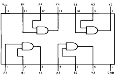
74LS08 AND Gate IC Pin Configuration
- Pin 1(A1): This is the first AND logic gate’s first input pin in the IC.
- Pin2 (B2): This is the first AND logic gate’s second input pin in the IC.
- Pin3 (Y1): This is the first AND logic gate’s output will be obtained at this pin.
- Pin4 (A2): This is the second AND logic gate’s first input pin within the IC.
- Pin5 (B2): This is the second AND logic gate’s second input pin within the IC.
- Pin6 (Y2): This is the second AND gate’s output pin in the IC.
- Pin7 (GND): This is a GND pin.
- Pin8 (Y3): This is the third AND logic gate’s output pin in the IC.
- Pin9 (A3): This is the first input pin of the third AND logic gate in the IC.
- Pin10 (B3): This is the second input pin of the third AND logic gate in the IC.
- Pin11 (Y4): This is the fourth AND logic gate’s output pin in the IC.
- Pin12 (A4): This is the fourth AND logic gate’s first input pin.
- Pin13 (B4): This is the fourth AND logic gate’s second input pin.
- Pin1 4 (VCC): This is the power supply pin, used to provide supply to the IC for making it functional.
Features & Specifications:
The features and specifications of 74LS08 AND gate IC include the following.
- 74LS08 AND gate IC has less power consumption.
- The operating speed of this IC is very fast.
- This logic gate IC is very small in size & also available in various packages like PDIP, SOP & SOIC.
- This IC operation is very simple and significantly cheaper.
- This IC uses a single power supply to turn ON all inbuilt logic gates.
- A single logic AND gate in the IC is used without affecting other gates.
- The output of this IC comes in TTL, so it is used to operate most of the microcontrollers & devices.
- The operating voltage range of this AND logic gate IC is 4.75V to 5.25 Volts.
- The recommended voltage of this IC must be 5V although this IC holds a voltage up to a maximum of 7V.
- The maximum current provided by this IC at its outputs is 8mAmps.
- The rise time and fall time of this logic gate IC is 18ns.
- The operating temperature of this IC ranges from 0 to 70 degrees although it also has the capability to store -65 to 150 degrees of temperature.
Equivalent & Alternative ICs
The equivalent 74LS08 AND gate ICs are; 74LS73, 74LS04, 74LS00, 74LS138, 74LS02, SN54LS08, HEF4081 & IC 7408. The alternative 74LS08 AND gate ICs are; 74×09, 74×7001 &CD408.
74LS08 AND Gate IC Circuit Diagram
The simple 74LS08 AND logic gate IC circuit diagram is shown below. This circuit can be built with AND logic gates, two push buttons, LED, resistor, and voltage supply. Give the connections as per the logic gate circuit shown below.
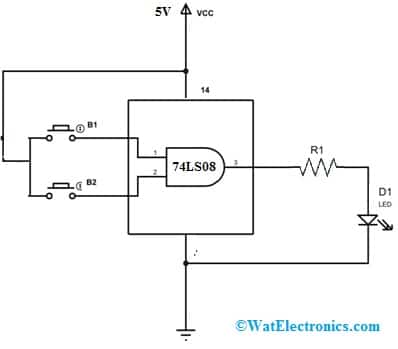
74LS08 AND Gate IC Circuit Diagram
Working
The two inputs of AND gate are connected to the two buttons for changing the inputs logic. The output of this gate is given to the LED through the ‘R1’ resistor. The LED in the circuit is connected to notice the output state.
The working of this circuit is, whenever both buttons in this logic circuit are not pushed, then the input of the logic gate will be zero, so the output will be zero and the voltage across the R1 resistor will be LOW, so it will make the LED to turn OFF. So when two inputs are LOW, then the output will be LOW.
In the second case, when any one of the buttons is pushed, then the inputs to the logic gate will be High and Low, so the output will be low. The voltage across the R1 resistor will be LOW which will make the LED turn OFF. So when one input is LOW, then the output will be LOW.
In the third case, when two push buttons are pushed, then the inputs to the logic gate will be High, so the output will be high. The voltage across the R1 resistor will be increased which will make the LED turn ON. So when two inputs are HIGH, then the output will be HIGH.
Once verifying the above three states, we can write the logic expression for AND logic gate using the truth table as; Y = A.B. In this way, we can utilize each logic gate in the IC based on the requirement.
Applications
The applications of 74LS08 AND Gate IC include the following.
- 74LS08 IC performs general-purpose AND gate logic.
- This AND logic gate IC is used in different devices like servers, digital electronics, memory units, networking devices, ALU, etc.
- This IC is used widely in various digital systems.
- This IC is used within digital electronics for data transmission control.
- This logic gate IC is used in alarm circuits.
Please refer to this link for 74LS08 AND Gate IC Datasheet.
Thus, this is an overview of 74LS08 AND logic gate IC, features, specifications, circuit, working, and its applications. This AND logic gate IC is known as QUADRUPLE 2 -input logic gate because this IC includes four AND logic gates wherever every logic gate is separately utilized without affecting other logic gates. Here is a question for you, what are the other AND logic gate ICs available in the market?