Imagine trying to build the world’s largest puzzle. Normally, when you make electronic chips, you cut a big silicon wafer into many small pieces (chips), package them, and connect them later. Wafer-Scale Integration (WSI) flips this idea — instead of cutting the wafer into smaller chips, engineers use the entire wafer as one giant chip. This sounds simple in words, but in reality, it is one of the most complex engineering challenges in the semiconductor world. Yet, it is also a revolutionary way to build AI superchips, like the ones made by Cerebras Systems, which are as big as a dinner plate!
This article will explain:
- What WSI is.
- Why do engineers want to use it?
- The step-by-step process of making such chips.
- The challenges and solutions.
- Why it matters for AI and supercomputers.
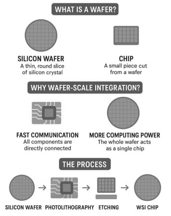
1. What is a Wafer?
A wafer is a thin, round slice of silicon crystal, like a pizza base.
- Diameter: ranges from 200 mm to 300 mm in modern fabs.
- Thickness: about 0.7 mm.
- The process serves as the canvas for creating billions of transistors.
Normal Way
- In traditional chip manufacturing, manufacturers cut the wafer into tiny chips, known as dies.
- Each die might be 1–2 cm².
- They then package each chip individually and connect them on circuit boards.
WSI Way
- However, in this innovative approach, the entire wafer—up to 300 mm wide—functions as a single chip.
- This method allows designers to place tens of thousands of cores side by side, establishing ultra-fast direct connections.
Think of it like baking a pizza:
- Normal chips = cutting the pizza into slices and eating one at a time.
- WSI = eating the whole pizza in one piece.
Wafer-Scale Integration (WSI)
2. Why Wafer-Scale Integration?
The main reasons are speed and efficiency:
1. Faster Communication:
- In normal chips, data travels between different packaged chips over wires.
- In WSI, everything is directly connected on silicon — like talking face-to-face instead of using a phone.
2. More Computing Power:
- A single WSI chip can pack hundreds of thousands of processing cores.
- Example: Cerebras WSE-2 has 850,000 AI cores.
3. Saves Energy:
- Less need for external connections and data movement.
- AI workloads, which need huge parallel operations, run more efficiently.
3. Step-by-Step Fabrication Process of Wafer-Scale Integration
Let’s walk through the process like building a giant city on one big island instead of many small ones.
Step 1: Silicon Wafer Preparation
- The Czochralski process grows a pure silicon crystal.
- Manufacturers then slice the crystal into thin wafers and polish them until they shine like mirrors..
- Each wafer becomes the foundation for the circuit.
(Analogy: Preparing the land before building a city.)
Step 2: Photolithography – Drawing the Circuits
- A thin film of photoresist (light-sensitive material) is spread.
- Light shines through a mask that has the circuit patterns.
- Wherever light hits, patterns are formed.
In WSI, instead of drawing patterns for just a small chip, engineers must design patterns for the entire wafer, covering hundreds of square centimeters.
(Analogy: Printing a whole city map on the land at once.)
Step 3: Etching and Doping – Creating Transistors
- Etching removes unwanted silicon parts.
- Doping adds tiny amounts of chemicals (like boron, phosphorus) to control how transistors conduct electricity.
- This process is repeated layer by layer to build billions of transistors.
(Analogy: Building houses, roads, and utilities across the whole city.)
Step 4: Interconnect Layers
- After transistors are built, they must be connected.
- Engineers deposit thin layers of metal (usually copper) to form wires.
- In WSI, there are tens of kilometers of wiring on a single wafer.
- Modern WSI chips use 14 or more metal layers.
(Analogy: Building highways and roads between neighborhoods in the city.)
Step 5: Handling Defects (The Hardest Part)
This is the biggest challenge in WSI.
- No wafer is perfect — some areas always have defects.
- In normal chips, defective dies are thrown away.
- But in WSI, you cannot throw away the wafer.
Solution: Engineers build redundant cores.
- If some cores fail, they are bypassed.
- The chip is still usable because thousands of extra cores are available.
(Analogy: If a few buildings collapse in the city, people just avoid them and live in others.)
Step 6: Power Delivery and Cooling
Another big challenge: a wafer-scale chip consumes tens of kilowatts of power.
- Power Delivery: Special packaging is designed to bring current into every part of the wafer evenly.
- Cooling: WSI chips use liquid cooling plates directly attached to the wafer. Air cooling is not enough.
(Analogy: Supplying water and electricity to every home in a megacity, and keeping the city cool in
summer.)
Step 7: Packaging
Unlike normal chips that are packaged individually:
- WSI chips are packaged as one giant piece.
- Engineers use custom connectors to link the wafer directly to external systems (like memory and servers).
This makes WSI packaging one of the most specialized in the world.
Key Innovations in Wafer-Scale Integration
- Redundancy: Extra cores and wires to handle defects.
- High-speed Mesh Networks: All cores are connected in a grid-like network.
- Advanced Cooling: Direct water/liquid cooling solutions.
- Custom Software: AI frameworks optimized to run on millions of cores.
5. Example: Cerebras Wafer-Scale Engine
- Size: 46,225 mm² (entire 300 mm wafer).
- Cores: 850,000 AI-optimized cores.
- Memory: 40 GB on-chip SRAM.
- Power: ~15 kW.
This single chip can replace dozens of GPU servers for AI training.
6. Challenges of WSI
- Manufacturing Defects – solved with redundancy.
- Yield – harder to achieve a high yield than with small dies.
- Cost – WSI chips cost millions to build.
- Software Support – needs special programming models.
- Cooling & Power Delivery – requires complex infrastructure.
Why WSI Matters for the Future?
- AI Training: Neural networks are getting larger, and traditional chips cannot keep up.
- Supercomputers: WSI could drastically reduce the size and cost of data centers.
- Scientific Research: WSI chips can model weather, physics, and genomics at unprecedented speed.
In short, WSI is a paradigm shift in chip design, moving from “small and many” to “big and unified.”
Wafer-Scale Integration is like building an entire city on a single island rather than scattering towns across different regions. It is difficult, expensive, and full of challenges — but it unlocks incredible power for AI and scientific computing.
Companies like Cerebras have shown that with smart design (redundancy, cooling, interconnects), WSI is not just possible but practical. You can also think of it like this:
- A normal microchip is like a classroom of students solving math problems.
- A WSI chip is like an entire school solving them together, with hallways (interconnects) connecting everyone instantly. To know further on how AI fabrication is done click here AI chip fabrication : step by step