Shift Registers are constructed using latches or the Flip-Flops. These Sequential circuits are used to generate certain delays in the digital waveforms or signals. To send data bits into the microprocessors/microcontrollers and for reading data out these, shift registers are used. The ‘n’ number of stages in the register is proportional to the delay generated in the circuit by n times. These registers play a vital role in long distance communication (like UART) between two processors to avoid the complexity of parallel wiring and its slow data transmission. To the conversion of data from parallel to serial, these registers are used.
What is Shift Register?
Shift Registers are the logic circuits of sequential type. These circuits are influenced by both present stage inputs and Past values. The basic purpose of these circuits is to store and transfer the data. The data stands for binary information. These registers are comprised of latches which are of D-type. The number of bits is directly proportional to the number of latches used. The formation of shift registers is dependent on the latches used. The most frequently used one is the register with eight bits. The data transfer or the data taken for storage can follow the process of parallel or serial both.
What are shift registers Used for?
These registers are used in computers and calculators. During the initial stages of arithmetic operation and to store the bits these devices are preferred. To convert the data from serial to parallel and vice-versa these registers are installed at the input or output side. The number of registers used are connected serially. This type of connection is also referred to as Daisy Chain Configuration.
In this type of connection, the output of the previous stage is provided as input to the register present at the next stage. These devices are powered up with a clock to achieve synchronous operation. There exist a Reset or the Clear option in these registers. In the data transfer operation, the bit is loaded into the register and then forwarded.
Types of Shift Registers, Counters & Truth Table, Code, and Applications
Based on the operating modes and the structure followed by input and output bits these registers are classified as
- Serial in and Serial out
- Serial in and Parallel out
- Parallel in and Serial out
- Parallel in and Parallel out
Serial in serial Out
The register in which the data is applied serially. That is one after another and the output is obtained in a similar manner. It indicates that the bit is inserted one at a time and the bit leaves are also one at a time.
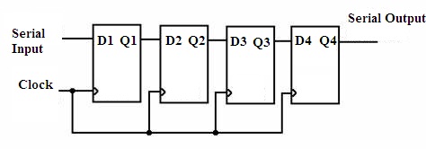
Shift Register (SISO)
Serial in parallel Out
The register for the purpose of the conversion of serial input into the parallel output. The input bits are applied one after another. But the output is obtained at once that is in a parallel manner.
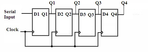
Shift Register (SIPO)
Parallel in Serial Out
The registers operated by applying the input bits in a parallel manner. All the bits are applied once at the input. But the output bits are obtained one after the other.
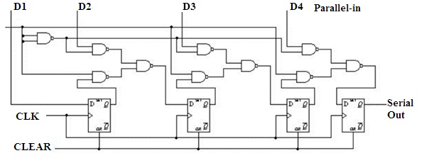
Shift Register (PISO)
Parallel in Parallel Out
In this mode of operation of these registers, the inputs are applied in a parallel manner. Simultaneously the output bits are obtained in the same manner.
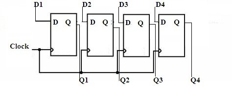
Shift Register (PIPO)
Bidirectional
This is a special case of the registers. This register is responsible for the operation of shifting bits in both the directions. Usually, there are two cases of shifting based on the direction that is left and Right.
If the value of the bit is shifted ‘left’ by one position resembles that the bit is multiplied by ‘2’. If the bit is shifted right by one position that is in equivalence to the bit divided by 2.
Among the two directions, one can be chosen based on modes in the single circuit. If the mode is set to high that is selected as 1 then the circuit operates as Right Shift Register. Similarly, the value of the mode is chosen as 0 the circuit operates as Left Shift Register.
Please refer to this link to know more about Shift Register MCQs
What are Universal Shift Registers?
This is a special case of shift registers. The registers are capable of loading and retrieving the data. It can be either in serial or parallel mode. By shifting the bits either left or right. The combination of ‘Unidirectional’ and ‘Bidirectional’ Registers with a Parallel Load provision can be referred to as Universal shift Registers.
please refer to this link for Universal Shift Register MCQs
Counters
Counters are one of the applications of shift registers. These are designed based on the serial input applied and output derived serially. The output of the last stage of the register is fed back to the first stage, forming a ring. The most widely used counters of this type are:
- Ring Counter
- Johnson Counter
Ring Counter
The basic type of counter designed by using D-Flipflops known as a Ring counter. Even this counter can be realized by using J-K flip-flops. The Flip-flops are arranged such that the output of one stage is fed back to the previous stage as input. But the output of the final stage that is Q is again fed back to the first stage flip-flop as input.
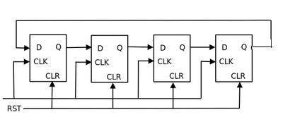
Shift Register (Ring Counter)
Johnson Counter
The realization of this counter is similar to the ring counter. A similar process of arrangement of flip-flops which is followed in the ring counter is followed. The only difference is the inverted output obtained at the final stage is fed back to the input at the first stage.
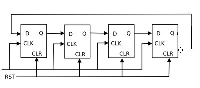
Shift Register (Johnson Counter)
But both the counters can suffer from a condition called ‘Lock-out’. This difficulty can be overcome by using an additional gate.
Further, there are various applications of shift registers. Some of them are listed as follows:
- The chain of Flip-flops connected together acts as a memory element. These are used in ‘Finite Memory Machines’.
- To generate Delays in the circuit these are preferred.
- To convert data from serial to parallel and parallel to serial. These registers are preferred.
The above are some of the applications of shift registers.
Verilog Code For Shift Register:
The below code is for a Shift Left Register of 8 bits ‘Serial In and Serial Out’ with a Positive edge.
module shift(clk, si, so);
input clk, si;
output so;
reg [7:0] tmp;
always @(posedge clk)
begin
tmp <= tmp<<1;
tmp[0] <=si;
end
assign so=tmp[7];
endmodule
Please check this article for How to Choose a Shift Register.
Please check this article for CD4014 Shift Register.
The Flipflops connected in the number of stages can be used for various purposes in the digital circuits. As per the name shift, the data bits are shifted for the purpose of transferring the data. This shift can be of two types either left, right or both based on the mode selected. Can you describe what is a Shift Right Register?