AI chips—like GPUs (e.g., NVIDIA’s H100) or custom accelerators—are marvels of precision engineering and materials science. Their manufacturing is an incredibly advancement of atomic-level manipulation, requiring unmatched cleanliness, extreme accuracy, and global coordination. Let’s explore the journey of AI chip fabrication from raw silicon to a powerful AI processor packaged and ready for deployment.
AI Chip Fabrication Process
The steps involved in AI chip fabrication include the following.
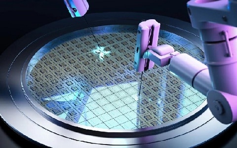
AI Chip Fabrication Process
1. Raw Materials & Wafer Preparation in AI Chip Fabrication
Silicon Purification
The journey begins with silicon, extracted from quartz sand and transformed into ultra-pure monocrystalline ingots. These are sliced into wafers—perfectly flat, flawless discs often 300 mm in diameter—with impurity levels so low they barely register even over global scales.
Cleaning & Oxidation
Each wafer is then thoroughly cleaned, polished, and often coated with a thin oxide layer to serve as a chemically inert starting surface..
2. Fabrication Pipeline: Front-End Processing
This phase includes all the steps through which the wafer becomes circuitry—commonly called front-end production.
Photolithography: Pattern Imprinting
- Wafers are coated with a photoresist.
- A photomask—holding the desired circuit pattern—is aligned on top.
- Light (often EUV at ~13.5 nm wavelength) exposes the photoresist in specific regions.
- The areas change chemically and are selectively removed or retained after development.
These steps are repeated dozens or even over 50 times, with each layer adding complexity to the final circuit.
Deposition & Etching
- Deposition lays down thin films—metals like copper for wiring or insulators (e.g., silicon dioxide).
- Etching selectively removes material to create the intricate patterns that define circuits.
- These build up the transistors and interconnects layer by layer.
Doping
To modify electrical properties, regions of the wafer are doped with impurities (e.g., phosphorus or boron), creating n-type or p-type zones necessary for transistor functionality.
Metrology & Inspection
At each step, metrology tools measure minute deviations to ensure precision. Specialized cameras, microscopes, and sensors detect defects early—some stages require repeating entire passes if issues are detected.
3. Enabling the Process: Equipment & Ecosystem in AI Chip Fabrication
Fabricating advanced AI chips requires the world’s most complex machinery:
- EUV lithography machines, especially those from ASML, are indispensable for sub-7 nm feature sizes. No competitor offers this capability.
- Major equipment providers like Applied Materials, KLA, Lam Research, Tokyo Electron, and ASML build the capital-intensive tools essential for chipmakers.
- The supply chain is intensely specialized and limited, making the fabrication of leading-edge chips extremely constrained geographically.
4. Design for Manufacturability (DFM)
As circuits scale down, any tiny imperfection can ruin functionality. DFM practices help designers anticipate manufacturing challenges by:
- Following strict geometrical rules from foundries.
- Using redundancy, optical proximity correction (OPC), and fill patterns to improve yield and reliability.
- Simulating process variability to mitigate defects early.
5. From Multiple Dies to One: Wafer-Scale & Advanced Packaging
Wafer-Scale Integration (WSI)
Innovators like Cerebras are creating truly massive chips—the wafer-scale engine—by integrating nearly an entire wafer into a single processor. It includes millions of AI cores and on-chip memory and designs around defects, so production yield is still high. To understand more on how Wafer Scale integration is done go through click on Wafer Scale Integrations process
Advanced Packaging & Chiplets
Instead of one massive die, modern AI chips often use chiplets: smaller dies interconnected in the same package. Techniques like 2.5D interposers and 3D stacking allow combining compute and memory die with high bandwidth and efficient pathways.
6. Backend Processing: Wafer Testing, Cutting, Packaging
Once front-end fabrication is done:
- The wafer is tested, and each processor (die) is marked as good or bad.
- Wafer is sawn into individual dies—defective ones discarded. Good dice are packaged—often via flip-chip techniques— and sent through final testing for performance, power, and reliability.
7. Role of Foundries & Global Production
Leading-edge AI chip fabrication is dominated by TSMC, Samsung, and Intel—with TSMC often regarded as the only facility reliably producing <7 nm chips for clients like NVIDIA, AMD, Apple.. Constructing and equipping an advanced fab costs tens of billions of dollars—TSMC alone is investing $100B over three years.. This high capital barrier restricts entry to very few players.
8. Yield, AI, & Quality Control
- Even at best, some manufacturing steps produce defects. To identify where issues arise:
- Companies like IBM Research use AI-driven algorithms to trace defect origins through hundreds of repeated process steps—catching issues early and avoiding wasted wafers.
9. From Fab to Future: Trends and Innovations
EUV is Key
Featuring prominently in modern fabs, EUV lithography machines are essential for fabricating transistors measured in nanometers—ASML leads this segment.
Edge & Specialized Chips
AI-specific designs (e.g., Cerebras wafer-scale chips) and novel architectures like thermodynamic computing ASICs are emerging, aimed at improving efficiency and performance.
10. AI Chip Fabrication Summary: From Sand to AI Silicon
|
Stage |
Purpose |
| Raw Materials | Purify silicon; slice wafers |
| Front End Fabrication | Pattern, etch, dope, deposit layers |
| DFM & Inspection | Ensure reliable manufacturable design |
| Packaging | Chop test |
| Foundry & Global Coordination | Build and run fabs; manage supply chain |
| Innovation | Wafer-scale chips, advanced packaging, AI in manufacturing |
The fabrication of AI chips stands at the intersection of extreme precision and advanced materials science. From purifying silicon to leveraging multi-billion-dollar machinery, the process demands global coordination, innovation, and exacting standards. As AI continues to scale, emerging technologies like wafer-scale integration, chiplet-based packaging, and novel architectures promise to redefine what’s possible.