FDV301N MOSFET is a semiconductor device that is used as a high-speed switching device in different applications. This is an N-Channel enhancement mode FET that is designed by using ON Semiconductor’s proprietary, DMOS technology & high cell density. The very high-density method is particularly adapted to reduce ON state resistance. This MOSFET is mainly designed for low-voltage applications as an alternative to digital transistors. So, this MOSFET replaces different digital transistors through different bias resistor values. This article discusses an overview of FDV301N MOSFET – pin configurations & their applications.
What is FDV301N MOSFET?
The FDV301N is a 3-pin N-channel MOSFET mainly used in low voltage & switching applications. This transistor carries low on-state resistance & replaces different types of transistors in a different range of applications. Generally, MOSFETs are divided into two types; P-channel MOSFET & N-channel MOSFET. In P-channel MOSFET, the majority of charge carriers are holes whereas, in N-channel MOSFET, the majority of charge carriers are electrons. The electron movement is better as compared to the hole movement, so N-channel MOSFET is better than P-channel MOSFET for various applications, particularly for high-load applications.

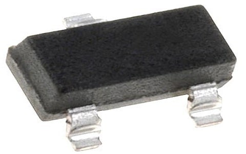
FDV301N MOSFET
FDV301N MOSFET Pin Configuration
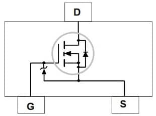
The symbol and pin configuration of FDV301N MOSFET is shown below. This MOSFET includes three terminals which are discussed below.

FDV301N MOSFET Pin Configuration
- Pin1 (Drain): The drain pin allows the flow of current to the device.
- Pin2 (Gate): Based on the applied voltage at this pin, this MOSFET gets turned ON & OFF. So, this pin is used for biasing the transistor.
- Pin3 (Source): The flow of current goes out throughout this pin. Usually, this pin is connected to GND.
Features & Specifications
The main features and specifications of FDV301N MOSFET include the following.
- FDV301 is an N-channel MOSFET.
- It is available in a SOT-23 surface-mount package made up of plastic or epoxy material, so its size is compact and weight is very less.
- This MOSFET is reliable & rugged.
- The type of channel is – N.
- The number of pins -3.
- The mode of the channel is Enhancement.
- The configuration of the transistor is single.
- Its length is 2.92mm.
- The material of the transistor is Si.
- Its width is 1.3mm.
- The Drain (D) to source (S) voltage or VDSS – 25V.
- The Gate (G) to source (S) voltage or VGSS – 8V.
- Input voltage or Vin – 5V.
- The threshold voltage from Gate (G) to source (S) or VGS th – 0.85V, 1.06V & 70V.
- The Drain current or ID – 22A.
- The dissipation of power or PD – 35W.
- The input capacitance or Ciss – 5pF.
- The output capacitance or Coss – 6pF.
- Junction temperature or TJ ranges from -55 to 150℃.
- Ambient thermal resistance – 357℃/W
- ON-state resistance or RDS(ON) – 4 to 5Ω.
- The rise time or tr ranges from 6 – 15ns.
- The total gate charge or Qg – 49 to 0.7nC.
- It has high cell density.
- It uses DMOS technology.
- It reduces on-state resistance.
- The voltage from the gate terminal to the source or VGS-th – is 8V.
FDV301N MOSFET Circuit Diagram
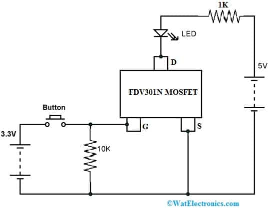
To understand the working of FDV301N MOSFET, let us consider a simple switching application circuit as given below. The simple switching circuit using FDV301N MOSFET is shown below. This circuit can be built with an FDV301N MOSFET, LED, two power sources 3.3V & 5V, and a button. In this switching circuit, the LED is used as a load.
In this circuit, two power sources are used (3.3V & 5V). The 5V power source is used to provide power to the load LED whereas the 3.3V power source is used to provide voltage to the gate terminal of FDV301N MOSFET. The function of the button is to turn ON the device.

FDV301N MOSFET Switching Circuit
Now let us consider the N-channel enhancement MOSFET characteristics because these characteristics will be applied to the MOSFET in this circuit. Generally, the MOSFET does not conduct once the voltage does not meet the threshold at the Gate to the Source junction.
The flow of current throughout Drain (D) is decided by the Gate (G) voltage up to a fixed point. Thus, if the Gate voltage is high then the MOSFET conduction resistance is low & the drain current is higher. In addition, this MOSFET conducts simply during the presence of voltage at the Gate terminal. If we remove the voltage at the Gate terminal immediately then the MOSFET will not conduct.
Similarly, when the button in the circuit is not pushed then there is no voltage at Gate, so the FDV301N MOSFET will not conduct the current. So MOSFET circuit acts as an open circuit due to the nonexistence of Gate voltage, so the whole supply voltage of +5V emerges across the device.
When the button is pushed immediately, then the +3.3V positive voltage appears at the gate terminal of the transistor, so the MOSFET will conduct. Once the MOSFET conducts, then the voltage will appear across the LED to turn it ON & it will wait in that condition till the button in the circuit is opened. So by using the button, the LED load will be turned ON & OFF.
In place of a button, we can also use the PWM of a microcontroller or other control signal within high-frequency applications. So in the above simple circuit, we have used FDV301N MOSFET as a switching device. Similarly, we can utilize the device in many other application circuits.
Applications
The applications of FDV301N MOSFET are discussed below.
- FDV301N MOSFET is applicable in different circuits like Battery management, DC-DC converter, Display driver, Low voltage & low current applications.
- This MOSFET is used in automotive electronics applications.
- It is used in High-speed switching & inverter applications.
- Servo motor control circuits.
- Power management functions.
- It is used in different memory circuits & also fundamental switching applications.
- It is used as a switching device within electronic control units, servo motor control & relay drivers.
- It is used in current electric vehicles as a power converter.
Please refer to this for How to Select a Transistor.
Please refer to this link to know more about IRFZ44N MOSFET Datasheet, FDV301N MOSFET Datasheet.
Thus, this is an overview of FDV301N MOSFET – pin configuration, specifications, circuit, and applications. These MOSFETs are available in extremely small sizes & can be developed & formed on a single Si (silicon) chip. The FDV301N is an N channel enhancement mode & SOT-23 surface-mount package logic level transistor. This single N channel MOSFET replaces different digital transistors through different bias resistor values. This transistor is appropriate for power management & low-voltage applications. Here is a question for you, what is the function of a MOSFET?