In CMOS (Complementary Metal-Oxide-Semiconductor) fabrication, well formation is a critical step that enables the integration of both NMOS and PMOS transistors on the same silicon substrate. The two main types of well technologies used are the n-well and p-well processes. Understanding the differences between these two approaches is essential for electronics engineers, VLSI designers, and students preparing for competitive exams like GATE or IES. This article explores the key differences between n-Well and p-Well CMOS Processes, fabrication flow, advantages, and real-world applications.
What is a Well in CMOS Fabrication?
A well is a region in the silicon substrate that is doped with either n-type or p-type impurities to allow the construction of the opposite type of MOS transistor:
- An n-well allows fabrication of PMOS transistors.
- A p-well allows fabrication of NMOS transistors.
In CMOS, both types of transistors are needed, so appropriate wells are formed to host each.
Why Are Wells Important?
CMOS technology requires NMOS and PMOS transistors to work together. Since both transistors require opposite doping types, wells are used to provide the necessary doping regions on a common substrate.
Fabrication Overview
This fabrication overview mainly includes the n-well CMOS process and the p-well CMOS process.
Differences Between N-Well and P-Well
n-Well CMOS Process
- Substrate: P-type silicon wafer
- Well formed: N-well
- NMOS: Built directly in the p-type substrate
- PMOS: Built in the n-well region
p-Well CMOS Process
- Substrate: N-type silicon wafer
- Well formed: P-well
- PMOS: Built directly in the n-type substrate
- NMOS: Built in the p-well region
Comparison Table: n-Well vs p-Well CMOS Process
The comparison between these two CMOS processes is discussed below.
|
Feature |
n-Well Process |
p-Well Process |
| Substrate Type |
P-type |
N-type |
| Well Formed |
N-well |
P-well |
| NMOS Transistor |
In substrate |
In p-well |
| PMOS Transistor |
In n-well |
In substrate |
| Technology Prevalence |
Widely used (especially in digital ICs) |
Less common in standard processes |
| Latch-Up Susceptibility |
Higher (due to p-substrate) |
Lower |
| Noise Immunity |
Lower |
Higher |
| Fabrication Simplicity |
Simpler, especially for PMOS tuning |
Simpler NMOS tuning |
| Performance (Speed) |
NMOS performs better |
PMOS performs better |
Detailed Differences between n-Well and p-Well CMOS Explained
1. Transistor Placement
- In an n-well, PMOS is placed in the n-well, and NMOS is directly in the p-type substrate.
- In the p-well, NMOS goes into the p-well, and PMOS remains in the n-type substrate.
2. Substrate Behavior
- P-type substrates (n-well process) are more prone to latch-up due to parasitic pnpn structures.
- N-type substrates (p-well process) reduce latch-up but are less commonly used.
3. Mobility Consideration
- Electron mobility (in NMOS) is higher than hole mobility (in PMOS), so NMOS often dominates performance.
- n-Well processes are optimized for NMOS in substrate → Better performance in digital circuits.
4. Noise Margin
- P-well provides better isolation for NMOS, hence better noise margin and stability in analog/mixed-signal designs.
5. Process Complexity
- n-Well processes are simpler when using a p-type wafer (which is the industry standard).
- p-Well processes require n-type substrates, which are less standard in CMOS fabs.
6. Cost and Scalability
- n-Well processes are more cost-effective and scalable for mass production.
- p-Well is suitable for applications where noise immunity and latch-up reduction are critical.
Read more: The Differences between NMOS and PMOS Technology.
Use Cases and Applications
n-Well CMOS is Ideal For:
- Digital ICs and Microprocessors.
- Memory Devices (SRAM, ROM).
- Low-power applications.
p-Well CMOS is Used In:
- Mixed-signal or analog circuits.
- High-reliability and automotive-grade ICs.
- Latch-up sensitive environments.
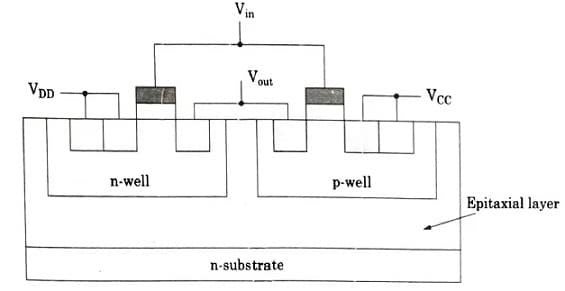
Moving Beyond: Twin-Well and Twin-Tub CMOS
To combine the best of both worlds, twin-well (or twin-tub) processes are used where both n-well and p-well are formed on the same substrate. This allows:
- Independent optimization of NMOS and PMOS.
- Better control over threshold voltages.
- Lower latch-up probability.
Read more: CMOS Fabrication: Process Steps and Twin-Tub Structure Explained
The difference between n-well and p-well CMOS processes lies in their substrate choice, transistor placement, latch-up behavior, and performance characteristics. While n-well is more common in digital VLSI, p-well provides advantages in analog and noise-sensitive applications. Understanding these distinctions is essential for anyone working in semiconductor design, fabrication, or electronics engineering.