The PWM boost converter allows for a variable input & stable output. So the output is controlled through the control circuit that adjusts the duty cycle of the gating pulse to maintain a stable output. The fundamental PWM boost converter switch has benefits like easy operation & easy control. There is a problem within closed-loop applications based on the variation of PWM techniques like the harmonics current & the voltage signal. This article elaborates on PWM boost converter IC namely LM2698 IC, pinout, features, specifications, and its applications.
What is LM2698 IC?
The LM2698 is a highly efficient synchronous PWM boost converter IC which is available in an 8-pin low-profile, VSSOP package. It is designed mainly for powering portable devices so this IC steps up (or) down an input voltage. This IC operates from 2.2 V to 12 V input voltages and provides output voltage from 2.2 V to 17 V. So the 1.9Amps, 18Volts, 0.2ohm internal switch allows this IC to give very efficient power conversion to outputs. It includes a 600 kHz (or) 1.25 MHz pin-selectable switching frequency that promotes flexibility in component selection & filtering methods whereas a shutdown pin reduces quiescent current supply to 5 µA.
Working
The LM2698 PWM boost converter IC works by efficiently changing power to outputs from 2.2 V to 17 V range. This IC operates from 2.2 V to 12 V input voltages and provides 12 V output at 400 mA. So this IC can be utilized in SEPIC or flyback topologies. This IC’s external compensation pin provides the user flexibility in frequency compensation setting to use very small and low-ESR ceramic capacitors at its output. Its current-mode architecture provides better line regulation, load regulation & simple frequency compensation.
LM2698 IC Pin Configuration:
The LM2698 IC pin configuration is shown below. So this IC includes 8 pins which are discussed below.
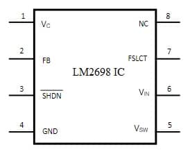
LM2698 Pin Configuration
- Pin-1 (VCC): It is the power supply pin of the IC that works below the applied voltage to it.
- Pin-2 (FB): It is an o/p voltage feedback input pin of IC.
- Pin-3 (SHDN): It is a shutdown control i/p, active low pin of IC.
- Pin-4 (GND): It is a power ground pin.
- Pin-5 (VSW): It is a power switch input pin where it is connected between SW & GND pins.
- Pin.6 (VIN): Analog input power pin.
- Pin-7 (FSLCT): It is a switching frequency select input pin where VIN= 1.25MHz and Ground = 600 kHz.
- Pin-8 (NC): It is a non-connected pin of IC.
Features & Specifications:
The features and specifications of LM2698 IC include the following.
- It is a general-purpose PWM boost converter IC.
- This IC includes 8 pins.
- It is available in the VSSOP package.
- This IC has a 1.9Amps, 0.2ohm internal switch.
- Its operating voltage is 2.2 V.
- Its adjustable frequency ranges from 600 kHz to 1.25 MHz.
- This IC supplies 12V output from a 5V input at 400 mA.
- Its operating junction temperature ranges from–40 to 125 °C.
- Its storage temperature ranges from −65˚C to +150˚Centigrade.
Equivalents & Alternatives:
Equivalents to LM2698 ICs are; LM2621, LM2700, LM5000, LM2623, etc. Alternatives to LM2698 ICs are; LM2672M-ADJ/NOPB and LM2672M-3.3.
Voltage Booster Circuit with LM2698 IC
The voltage booster circuit is used to enhance the input voltage at the load connected to the output. As the name suggests, the input voltage it takes and transforms into high voltage using some electronic components. This circuit is designed with different methods like capacitors, inductors, semiconductor switches, and many more. However, some voltage regulator chips can also be available in the market to provide efficient output. Thus, we are designing a 12V voltage booster circuit with LM2698 IC.
The required components to make this circuit mainly include; an LM2698 IC, a pin connector, a 10µH inductor, 0MQ040N diode, capacitors like 4.7nF, 10µF, and 22µF, resistors like; 30.1K, 3.48K, and 24.9K. So connect this circuit as per the circuit diagram shown below.
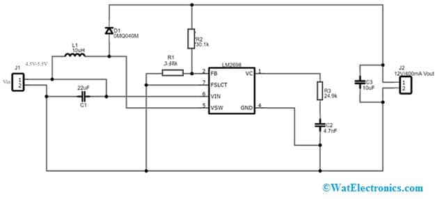
Voltage Booster Circuit with LM2698 IC
Working
This voltage booster circuit has an 8-pin LM2698 IC. The input voltage can be given at pin-6 (VIN) of a chip whereas pin-4 of this IC can be used for GND. Here, pin 5 of the IC is the analog power input switch. Pin-1 is used for the compensation network connection, so it is connected to the o/p of the voltage error amplifier.
Thus, pin-2 is the input pin for the output voltage feedback. Once all these connections are made, the input voltage is provided to the circuit which ranges from 4.5V to 5.5V. After that, this circuit changes this voltage to 12V and provides the output. Any load can be connected that requires 12V and draws 400mA of maximum current.
Thus, this circuit can be utilized as a boost converter. In addition, it is used in the distributed power supply. So, it is used in any electronic circuit that needs to change 5Volts to 12Volts.
Advantages & Disadvantages
The advantages of LM2698 IC include the following.
- A PWM boost converter maintains a stable output when the input changes.
- It provides precise control above the converter’s output voltage.
- These are very efficient, particularly when the voltage difference is small.
- This IC can step up (or) step down an input voltage.
- It has a low input current ripple.
- This boost converter IC sets the power density standard
- This IC provides efficient power change to outputs
- This IC’s shutdown pin decreases the quiescent current supply to 5 µA.
The disadvantages of LM2698 IC include the following.
- Its quick current switching can produce high levels of EMI.
- The load may generate audible noise.
- PWM can be difficult in some applications like motor control, and sensor feedback synchronization, PWM needs precise timing, etc.
- Component stress can lead to many issues; high current ripple within the input inductor, output diodes reverse recovery, high voltage ripple within the output capacitors, etc.
- PWM enhances switching frequency, so it can decrease the life span of the power device & also switching losses can be increased.
- PWM can cause difficult effects on the load like current ripples, torque pulsations, voltage spikes, acoustic noise, etc.
- It needs a high-performance controller & driver circuit, so it increases the price & the converter’s complexity.
- The boost converter switch causes an RHP zero, thus the output firstly drops whenever the switch is ON for a longer period.
- The voltage gain is limited by the sum of energy that should be stored temporarily before it is transmitted from the i/p to the o/p side.
Applications
The applications of LM2698 IC include the following.
- The LM2698 IC is used for power conversion from 3.3 V to 5 V & 5 V to 12 V.
- This IC can be used within DSL modems, set-top boxes, and diagnostic medical instrumentation.
- This IC can be utilized in boost converters, Flyback & SEPIC converters.
- It can be used for power distribution.
Please refer to this link for the LM2698 IC Datasheet.
Thus, this is an overview of LM2698 IC, pin-out, features, specifications, circuit, working, pros, cons, and its applications. So this is a general-purpose PWM boost converter IC that provides very efficient power conversion to the range of outputs from 2.2 V to 17 V. Its operating voltage ranges from 2.2 V to 12 V. Its current-mode architecture provides load regulation, superior line regulation & easy frequency compensation. Thus, here is a question for you, what is LM2700 IC?