The increasing complexity of modern embedded systems and System-on-Chip (SoC) designs demands an efficient and standardized method for communication between internal components such as processors, memory units, and peripheral devices. As the number of integrated modules grows, the need for a well-defined on-chip interconnect becomes critical to ensure reliable data transfer, scalability, and design efficiency. To address this requirement, Arm Holdings introduced the Advanced Microcontroller Bus Architecture (AMBA Bus Architecture). AMBA is not merely a bus standard; it defines a complete communication protocol framework that governs how transactions are initiated, transferred, controlled, and completed between different components in a system.
The strength of AMBA lies in its layered design approach. It separates high-performance data movement from low-speed control communication by introducing multiple protocols—AXI, AHB, and APB—each optimized for a specific role. To truly understand the AMBA bus architecture, one must move beyond block diagrams and focus on how messages are formed and how they physically move through the system over time.
AMBA Bus Architecture: Structural and Functional View
At a structural level, AMBA organizes the SoC into three interacting domains: the high-performance interconnect, the system-level bus, and the peripheral interface. However, the real essence of the architecture lies in how these domains cooperate during a transaction.
When a processor needs to read or write data, it does not directly “access memory” in a simple sense. Instead, it generates a transaction request, which is interpreted and routed by an interconnect fabric. This fabric determines the destination slave device based on the address and manages contention if multiple masters request access simultaneously.
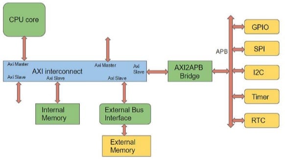
AMBA Architecture Diagram
In high-performance systems, this interconnect is typically based on AXI, which allows multiple transactions to be active concurrently. In simpler systems, AHB provides a shared communication medium where transactions are pipelined but still centrally controlled. For low-speed peripherals, APB acts as a simplified extension, with deterministic, minimal communication. Thus, AMBA is best understood as a transaction-routing and execution system, rather than just a bus.
Fundamental Communication Model in AMBA Bus Architecture
Every communication in the AMBA bus architecture follows a structured sequence:
- Transaction initiation by a master
- Address phase to identify the target slave
- Data transfer phase
- Response phase indicating completion status
Unlike traditional buses, where these steps occur sequentially and tightly coupled, AMBA protocols—especially AXI—allow these phases to be decoupled and overlapped, significantly improving performance.
The way these phases are implemented varies across AXI, AHB, and APB, and these differences define their performance and complexity.
AXI Protocol: Message Format and Data Transfer
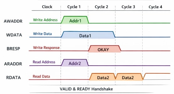
AXI Protocol Timing
Conceptual Foundation
AXI is designed as a fully decoupled, multi-channel communication protocol. Instead of sending all information through a single pathway, AXI divides a transaction into independent channels. This separation allows different parts of the transaction to proceed simultaneously.
This is the key reason AXI achieves high throughput—it removes unnecessary dependencies between address, data, and response phases.
AXI Message Format
An AXI transaction is not a single packet but a combination of signal groups transmitted over five channels:
- Write Address Channel
- Write Data Channel
- Write Response Channel
- Read Address Channel
- Read Data Channel
Each channel carries a specific portion of the transaction message.
For example, a write operation consists of:
- An address message (where to write)
- A data message (what to write)
- A response message (status of write)
These are transmitted independently.
AXI Write Transaction: Detailed Operation
When a master initiates a write operation, it first sends the write address through the address channel. This includes not just the memory location but also additional attributes such as burst length and transfer size.
Importantly, the data does not have to wait for the address to be complete. The master can begin sending data through the write data channel as soon as it is ready. This decoupling allows the address and data phases to overlap or even occur out of order in complex systems.
The slave, upon receiving both address and data, processes the write and returns a response through the write response channel. This response confirms whether the operation was successful or if an error occurred.
AXI Read Transaction: Detailed Operation
In a read operation, the master sends the read address through the read address channel. The slave then retrieves the requested data and returns it through the read data channel.
If the transaction involves multiple data words (burst transfer), the slave sends multiple data beats sequentially. Each beat may be accompanied by status information, and the final beat indicates completion.
Handshake Mechanism (VALID–READY)
One of the most critical aspects of AXI is its handshake mechanism.
Every channel uses two signals:
- VALID: Indicates that data is available
- READY: Indicates that the receiver can accept data
A transfer occurs only when both signals are asserted simultaneously.
This mechanism ensures that:
- Data is never lost
- Slow components can stall fast ones safely
- System operates reliably under varying conditions
Implication of AXI Design
The independence of channels and handshake-based flow control allows:
- Multiple transactions are to be active simultaneously
- Out-of-order execution
- High bus utilization
This is why AXI is used in high-performance systems such as CPUs, GPUs, and AI accelerators.
AHB Protocol: Message Format and Data Transfer
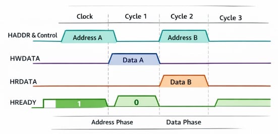
AHB Protocol Timing Diagram
Conceptual Foundation
AHB represents an intermediate step between simple buses and advanced interconnects. It introduces pipelining, allowing overlapping of address and data phases, but retains a shared bus architecture. This means that while performance is improved compared to simple buses, it still has limitations in scalability.
AHB Message Format
Unlike AXI, AHB uses a single combined channel for address and control signals.
Message Format
A typical AHB message includes:
- Address (HADDR)
- Control signals (HTRANS, HWRITE, HSIZE)
- Data (HWDATA or HRDATA)
- Response (HRESP)
- Ready signal (HREADY)
All these signals work together to define and complete a transaction.
AHB Data Transfer Mechanism
AHB divides each transfer into two phases:
- Address phase
- Data phase
The key optimization is that these phases are pipelined.
While data for one transaction is being transferred, the address for the next transaction can be issued. This overlap increases throughput without requiring multiple channels.
Detailed Operation
- When a master initiates a transaction, it places the address and control signals on the bus. In the next clock cycle, the data corresponding to that address is transferred.
- At the same time, the next address can already be placed on the bus. This creates a pipeline where each stage is continuously active.
- However, if the slave is not ready, it can hold the HREADY signal low, inserting wait states. This pauses the pipeline until the slave is ready to continue.
Implication of AHB Design
AHB improves efficiency through pipelining, but still suffers from:
- Bus contention (only one master active at a time)
- Limited scalability
It is therefore suitable for medium-performance systems.
APB Protocol: Message Format and Data Transfer
Conceptual Foundation
APB is designed with a completely different philosophy: simplicity and low power. It eliminates pipelining and complex control mechanisms to create a deterministic and easy-to-implement interface.
APB Message Format
APB uses a minimal set of signals:
- Address (PADDR)
- Write control (PWRITE)
- Data (PWDATA / PRDATA)
- Enable signal (PENABLE)
- Select signal (PSEL)
These signals define a complete transaction.
APB Transfer Mechanism
- APB communication occurs in two distinct phases.
- In the first phase (setup), the master places the address and control signals on the bus and selects the target slave. No data transfer occurs at this stage.
- In the second phase (access), the enable signal is asserted, and the actual data transfer takes place.
- This two-step process ensures predictable timing and eliminates the complexity of pipelining.
Implication of APB Design
APB is:
- Simple to design
- Low power
- Deterministic
But it is also:
- Slow
- Not suitable for high data throughput
Hence, it is used for peripherals like UART, GPIO, and timers.
Key Differences at Message Level
|
Feature |
AXI | AHB |
APB |
|
Channels |
5 independent | Single | Single |
|
Message Type |
Transaction-based | Pipelined | Simple |
|
Handshake |
VALID/READY | HREADY |
PENABLE |
| Burst | Yes | Yes |
No |
| Parallelism | High | Medium |
None |
AMBA Interconnect and Message Routing
- In a real SoC, transactions rarely occur in isolation. Multiple masters may simultaneously request access to multiple slaves. The interconnect is responsible for routing these transactions correctly.
- In AXI-based systems, the interconnect acts like a switch, allowing multiple data paths to exist simultaneously. In AHB systems, an arbiter decides which master gets access to the shared bus.
- When a transaction targets a peripheral, it is routed through a bridge that converts the high-speed protocol into APB format. This ensures compatibility while maintaining system efficiency.
Conclusion
AMBA bus architecture is fundamentally a transaction-oriented communication framework that enables efficient data exchange in modern SoCs. AXI, AHB, and APB represent different design trade-offs between performance, complexity, and power.
AXI achieves high performance through channel decoupling and parallelism. AHB balances performance and simplicity through pipelining. APB prioritizes simplicity and low power through a minimal, deterministic interface.
Understanding AMBA at the level of message formats and data transfer mechanisms provides deeper insight into how modern embedded systems operate internally and is essential for anyone working in VLSI design, embedded systems, or hardware architecture.