Integrated circuits (ICs) power everything around us — smartphones, laptops, electric vehicles, satellites, and even medical equipment. But how does a digital circuit become a real silicon chip? This transformation happens during Physical Design (PD) in VLSI. Physical Design (PD) is the process of transforming a synthesized gate-level netlist into a manufacturable IC layout that meets performance, power, and area requirements while obeying foundry design rules. The output of physical design is typically a GDSII file, which is sent to the semiconductor foundry for fabrication.
Unlike logical design, physical design is heavily constrained by:
- Geometry and layout rules
- Interconnect delays
- Power delivery limitations
- Process variations
- Manufacturability concerns
Because of these constraints, PD is highly iterative and optimization-driven.
Position of Physical Design in the VLSI Flow
The typical VLSI flow is:
- Specification
- RTL Design
- Functional Verification
- Logic Synthesis
- Physical Design
- Physical Verification
- Tape-out
- Fabrication
Physical design begins after synthesis, using:
- Gate-level netlist
- Timing constraints (SDC)
- Standard cell libraries (LEF/Lib)
- Power intent (UPF/CPF)
Inputs and Outputs of Physical Design
Inputs:
- Synthesized netlist (Verilog)
- Timing constraints (SDC)
- Technology LEF
- Standard cell LEF
- Liberty timing files (.lib)
- Power intent files (UPF/CPF)
Outputs:
- GDSII layout database
- DEF (placement and routing)
- Timing reports
- Power reports
- DRC/LVS clean signoff reports
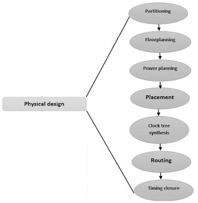
Physical Design Flow Overview
The major stages of physical design are:
- Floorplanning
- Power Planning
- Placement
- Clock Tree Synthesis (CTS)
- Routing
- Timing Closure
- Physical Verification & Signoff
Each stage strongly affects the next, making early decisions extremely important.
Physical Design in VLSI
Floorplanning
Floorplanning defines the physical structure of the chip. Key decisions include:
- Die size and shape
- Core area and utilization
- Macro placement
- IO placement
- Aspect ratio
Importance of Floorplanning
It is often said that 80% of PD success is decided during floorplanning. Poor macroplacement can cause:
- Severe routing congestion
- Timing bottlenecks
- IR drop issues
- Unfixable DRC violations
Macros, such as SRAMs and IP blocks, are placed early because they are fixed in size and consume block routing resources.
Power Planning
Power planning ensures reliable delivery of power and ground to all cells. It includes:
- Power rings
- Power straps
- Power grids
- Multiple voltage domains
Key Concerns:
- IR drop
- Electromigration (EM)
- Power gating
Upper metal layers are typically used for power routing due to their lower resistance and higher current-carrying capability.
Placement
Placement assigns physical locations to standard cells within the core area.
Types of Placement:
- Global placement (optimizes wirelength, congestion, timing)
- Legalization (removes overlaps, aligns rows)
- Detailed placement (local optimizations)
Key placement goals:
- Minimize wirelength (HPWL)
- Reduce congestion
- Improve timing
- Maintain legal placement constraints
Clock Tree Synthesis (CTS)
CTS is one of the most critical stages in the physical design process. Its goal is to:
- Distribute the clock signal
- Minimize skew and latency
- Balance insertion delay
Key CTS Concepts:
- Clock skew
- Clock latency
- Useful skew
- Clock buffering
- Clock shielding
CTS often introduces a large number of buffers, increasing power consumption but improving timing reliability.
Routing
It connects all placed cells using metal interconnect layers.
Routing Stages:
Global Routing
- Estimates the routing demand
- Identifies congestion hotspots
Detailed Routing
- Assigns exact tracks and vias
- Produces final wire geometries
Routing must handle:
- Signal integrity
- Antenna effects
- Design rule constraints
Timing Analysis and Closure
Static Timing Analysis (STA)
STA is a vectorless method used to verify timing across all paths.
Timing Violations:
- Set up violations (data arrives late)
- Hold violations (data arrives too early)
Corners:
- Slow-Slow (worst for setup)
- Fast-Fast (worst for hold)
Timing closure is achieved when setup and hold constraints are met across all corners.
Signal Integrity and Power Integrity
Signal Integrity Issues:
- Crosstalk
- Noise coupling
- Delay variation
Power Integrity Issues:
- IR drop
- Ground bounce
- Electromigration
Mitigation techniques include shielding, wider metals, via arrays, and decoupling capacitors.
Physical Verification
Before tape-out, the design must pass:
- DRC (Design Rule Check): Ensures manufacturability
- LVS (Layout vs Schematic): Ensures connectivity correctness
- ERC (Electrical Rule Check): Ensures electrical safety
Failure at this stage means the design cannot be fabricated.
Signoff and Tape-out
It ensures the design is safe for manufacturing under worst-case conditions. Signoff checks include:
- Timing signoff
- Power signoff
- EM/IR signoff
- DRC/LVS clean reports
Once tape-out occurs, photomasks are generated, and the design becomes irreversible.
Importance of Physical Design Skills
Physical Design engineers must balance:
- Power
- Performance
- Area
- Reliability
- Manufacturability
With advanced nodes (7nm, 5nm, 3nm), PD complexity continues to grow, making strong fundamentals essential.
FAQ
1: What is Physical Design in VLSI?
Physical Design (PD) in VLSI is the process of converting a synthesized gate-level netlist into a manufacturable IC layout. It focuses on optimizing power, performance, and area (PPA) while meeting timing, signal integrity, and fabrication rules.
2: What are the main stages in the Physical Design flow?
The main stages of Physical Design are:
- Floorplanning
- Power planning
- Placement
- Clock Tree Synthesis (CTS)
- Routing (global and detailed)
- Timing closure
- Physical verification (DRC, LVS, ERC)
- Signoff and tape-out
- Each stage strongly impacts the final chip quality.
3: Why is floorplanning considered the most critical PD stage?
Floorplanning determines die size, core utilization, macro placement, and routing channels. Poor floorplanning can cause congestion, timing violations, IR drop issues, and may become impossible to fix later, making it the most impactful stage in Physical Design.
4: What is Clock Tree Synthesis (CTS) and why is it important?
Clock Tree Synthesis (CTS) is the process of distributing the clock signal to all sequential elements with minimal skew and controlled latency. CTS is critical because clock skew directly affects setup and hold timing, overall performance, and chip reliability.
5: What is the difference between setup and hold violations?
- A setup violation occurs when data arrives too late before the clock edge.
- A hold violation occurs when data arrives too early after the clock edge.
Setup violations are worst in slow process corners, while hold violations are worst in fast corners.
Conclusion
In summary, the Physical Design is where theory meets silicon reality. A deep understanding of PD concepts is essential for building high-performance, low-power, and reliable chips. From floorplanning to signoff, every decision has long-lasting consequences.