In the domain of electronics, we know that a regulator is a type of device or apparatus that can control the level of output power. There are many kinds of regulators available in the market which depends on the supply of power. But primarily, in the conversion process of DC to DC, there are mainly two kinds of regulators which are Linear and Switching. A linear type of regulator adjusts the output through a resistive voltage drop. With this, efficiency decrement and also power loss in the form of heat can be occured. In switching regulators, they use an inductor, diode, and power switches for energy transmission from source to destination. In the same scenario, a flyback converter is a switching regulator which is more in the choice of many designers. And here this article explains flyback converter working, design, topology, construction, and applications.
What is Flyback Converter?
A flyback converter is employed for both the purposes of AC to DC and DC to DC conversions using galvanic isolation in between the input and the output. This device is termed a buck-boost converter having the inductor divided into the transformer and because of this, the voltage proportions are multiplied with the added benefit of isolation. The flyback converter topology is employed where numerous outputs are required to generate one output supply. Along with this, the topology permits the designers to alter the output polarity which means that there can be the creation of either +4V, +8V, and -7V levels of output from the one converter module. There can be enhanced efficiency rates in both situations.
The other feature in the flyback converter is electrical isolation for both the input and output. Isolation is needed in order to reduce the noise level and for some safety-related activities.
Operation of Flyback Converter
The device comprises the flyback transformer, rectifier, filter, and switch. It even contains a controlling process to simulate the switch and provides regulation. This is the lower section count switching type of converter and correspondingly simple to construct. Also, a flyback converter is an isolated kind of switching converter which can be either step-up or step-down.
Flyback Transformer
In general, a transformer has the functionality of transmission of energy from the primary winding to secondary winding perfectly and in real-time. Whereas a flyback transformer accumulates energy in its primary magnetic field and then after a specific period of time the energy gets transferred to the secondary winding.
Switch
The main functionality of the switch is to flip around ON and OFF conditions that correspond to the ability of the primary circuit to either magnetize or demagnetize the flyback transformer. This switch is regulated by the PWM signal that is receiving from the chosen controller.
Filtering and Rectification
Here, the voltage rectification is done by the rectifier on the secondary winding of the transformer which makes a pulsating type of DC. The other functionality of either the diode or rectifier is to cut down and then connect the load section from the secondary winding. This rectified voltage is then filtered using the capacitor where augments the DC level and it can be applied for the desired application. In many scenarios, a flyback converter required a snubber circuit where this tries to eliminate the voltage across those are generated across diode or switch.
Before knowing the operation, let us know what components are involved in the construction of the flyback converter.
Working Principle
The operation of the flyback converter can be explained in two conditions which are:
- Switch ON
- Switch OFF
Operation when Switch is ON
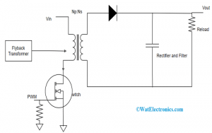
The flyback converter design when the switch is in ON condition is shown below:
Working of Flyback Converter in Switch ON
The operation of the flyback converter is mainly based on the switch operation. When the switch is in ON state, there will be the flow of current from Vin downwards to the primary and then to the ground. This tends to the accumulation of energy into the primary winding. At the time of this, there will be no current flow in the secondary winding because the diode is in reverse biased condition. In this condition, the load demand will be delivered by the output capacitance which is Cout. The derivation is shown below.
To be precise, a flyback converter functions to accumulate and transfer energy. When the switch is in ON condition, the primary winding of the transformer gets charged and current flow takes place. So, by the application of Kirchhoff’s law,
Vin -VL – Vs = 0
In the ideal scenario, the voltage drop is ‘0’ at this condition and
Vin – VL = 0, so Vin = VL
VL = Lp (di/dt)
di = (VL/Lp) dt
As Vin = VL, we get
di = (Vin/Lp) dt
With the application on integration to the above formula, we get
Ipri = ʃ0TON (Vin/Lp) dt
= ipri = (Vin/Lp) TON
When the equation is expressed in the form of accumulated energy, then
Epri = (1/2)ipri2Lp
= (1/2) ](Vin/Lp).TON]2Lp
Here, Vin corresponds to the input voltage of the primary winding
Lp corresponds to the transformer’s primary inductance
TON is the time considered at the time of switch ON condition
Operation when Switch is OFF
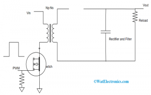
The flyback converter design when the switch is in OFF condition is shown below:
Operation of Flyback when the Switch is OFF
When the initial switch is in a cut-off state, the primary winding of the transformer withstands to a quick change in the current and the polarity of the winding gets reversed. This tends for forward biasing of the output diode. The accumulated energy in the primary winding will get transferred to the secondary winding and then to the load section through the diode. At this condition, the output capacitor tends to gain its charge.
When the switch is in OFF condition, the focus is mainly on the secondary winding of the transformer and there is current flow in this. So, by the application of Kirchhoff’s law,
VLsecondary– Vs – Vout = 0
In the ideal scenario, the voltage drop is ‘0’ at the secondary diode
VLsecondary – Vout = 0, so VLsecondary = Vout
VL = Ls (di/dt)
di = (VLsecondary/Ls) dt
As VLsecondary = Vout, we get
di = (VLsecondary /Ls) dt = (Vout /Ls) dt
With the application on integration to the above formula, we get
Isec = ʃTTON (Vsec/Ls) dt
= isec = (Vsec/Ls) (T – TON)
When the equation is expressed in the form of transferred energy, then
Esec = (1/2) ](Vsec/Ls).(T – TON)]2Ls
Here, Vsec corresponds to the input voltage of the secondary winding
Ls corresponds to the transformer’s secondary inductance
TON is the time considered at the time of switch ON condition
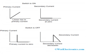
Waveforms of Flyback Converter Operation
This is the detailed principle of working and flyback converter design calculations.
Flyback Converter SMPS
The main usage of the device is in SMPS circuits. The above diagrams show the SMPS flyback converter design using a flyback transformer and a MOSFET switch. Here, in the device operation at any provided power level, it consists of the lowest components of the SMPS topologies. The provided supply can be of alternating or direct current. When the device is configured to operate using an AC line, there usually happens a full-wave rectification. The input is DC.
The main functionality lies in the flyback transformer. Differing to the general type of transformer windings, the flyback transformer will not carry current at both the windings at the same time period, this is because of the reverse indication of the winding phase as represented by the dot on windings and series diode on the secondary location.
There are many benefits to this SMPS topology. The primary usage is that the primary and secondary sections of the supply are isolated in an electrical way. This minimizes the transient coupling thus eliminating ground loops and provides enhanced flexibility at the output. The transformer permits various output voltages to be developed in the supply and extra windings for every voltage gets added up. Regulation is dependent on the single output whereas secondary outputs are normally regulated.
Limitations
The flyback converter faces a few limitations when operated in continuous and discontinuous modes and those are:
- The voltage feedback loop needs a minimal bandwidth because of the right-sided half plane zero in the response of the converter
- There has to be slope compensation in the conditions when the duty cycle is more than 50%
- As the power switches are operated with positive current flow, the switches turn-on speed is also crucial in order to minimize waste heat in the switching component
- There will be a peak level of currents, RMS, and flux excursions in the inductor.
Applications
The flyback converter applications are as follows:
- Used mainly in SMPS circuits which are like mobile chargers, standby supplies in computers, and in many others.
- Used in minimal-priced output power supplies which are personal computers less than 250 watts
- Employed for high range of voltage supply for oscilloscopes in monitors and televisions
- Used for the applications that need a high level of voltages such as lasers, photostat machines, xenon type of flash lamps, and others
- Isolated gate drivers
- Solar type of microinverters
- Used in telecom departments
- LED lights
- Power over Ethernet applications
This is all about a flyback converter. This article has provided a detailed analysis of flyback converter design, operation, using SMPS, and the applications of the device. To have a clear analysis on the topic, know what are the real-life examples of flyback converter and how they are operated?